

 Manufacturers
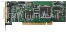
PORTWELL PCI-DA12-6

Description
Six Channel Analog Output with independent double-buffered, 12-bit D/A and 16-bits buffered digital I/O on a universal 3.3/5V powered half-sized PCI Card
Part Number
PCI-DA12-6
Price
Request Quote
Manufacturer
PORTWELL
Lead Time
Request Quote
Category
I/O Products
Specifications
Categorization Information
IO Products
Features
- Universal PCI, PCI-X, 3.3V and 5V compatible
- Six, 12-Bit, double-buffered, digital-to-analog converters
- Program control provides means for either individual update or simultaneous update of the DACs. can use an external signal in this way
- Unique, automatic control of DAC outputs to prevent spurious outputs at power-on
- 16-bits digital I/O buffered with tri-stateable transceivers
- Resettable-fused +5VDC available for external use
Datasheet

Extracted Text
MODEL PCI-DA12-2/4/6 USER MANUAL FILE: MPCI-DA12-6.A1m Notice The information in this document is provided for reference only. Portwell does not assume any liability arising out of the application or use of the information or products described herein. This document may contain or reference information and products protected by copyrights or patents and does not convey any license under the patent rights of Portwell, nor the rights of others. IBM PC, PC/XT, and PC/AT are registered trademarks of the International Business Machines Corporation. Printed in USA. Copyright 2000, 2005 by Portwell I/O Products Inc. All rights reserved. WARNING!! ALWAYS CONNECT AND DISCONNECT YOUR FIELD CABLING WITH THE COMPUTER POWER OFF. ALWAYS TURN COMPUTER POWER OFF BEFORE INSTALLING A CARD. CONNECTING AND DISCONNECTING CABLES, OR INSTALLING CARDS INTO A SYSTEM WITH THE COMPUTER OR FIELD POWER ON MAY CAUSE DAMAGE TO THE I/O CARD AND WILL VOID ALL WARRANTIES, IMPLIED OR EXPRESSED. Manual PCI-DA12-2/4/6 2 Warranty Prior to shipment, Portwell equipment is thoroughly inspected and tested to applicable specifications. However, should equipment failure occur, Portwell assures its customers that prompt service and support will be available. All equipment originally manufactured by Portwell which is found to be defective will be repaired or replaced subject to the following considerations. Terms and Conditions If a unit is suspected of failure, contact Portwell' Customer Service department. Be prepared to give the unit model number, serial number, and a description of the failure symptom(s). We may suggest some simple tests to confirm the failure. We will assign a Return Material Authorization (RMA) number which must appear on the outer label of the return package. All units/components should be properly packed for handling and returned with freight prepaid to the Portwell designated Service Center, and will be returned to the customer's/user's site freight prepaid and invoiced. Coverage First Three Years: Returned unit/part will be repaired and/or replaced at Portwell option with no charge for labor or parts not excluded by warranty. Warranty commences with equipment shipment. Following Years: Throughout your equipment's lifetime, Portwell stands ready to provide on-site or in-plant service at reasonable rates similar to those of other manufacturers in the industry. Equipment Not Manufactured by Portwell Equipment provided but not manufactured by Portwell is warranted and will be repaired according to the terms and conditions of the respective equipment manufacturer's warranty. General Under this Warranty, liability of Portwell is limited to replacing, repairing or issuing credit (at Portwell discretion) for any products which are proved to be defective during the warranty period. In no case is Portwell liable for consequential or special damage arriving from use or misuse of our product. The customer is responsible for all charges caused by modifications or additions to Portwell equipment not approved in writing by Portwell or, if in Portwell opinion the equipment has been subjected to abnormal use. "Abnormal use" for purposes of this warranty is defined as any use to which the equipment is exposed other than that use specified or intended as evidenced by purchase or sales representation. Other than the above, no other warranty, expressed or implied, shall apply to any and all such equipment furnished or sold by Portwell. Manual PCI-DA12-2/4/6 3 Table of Contents Chapter 1: Introduction................................................................................................. 5 Specifications ............................................................................................................ 6 Figure 1-1: Block Diagram ...................................................................................... 8 Chapter 2: Installation................................................................................................... 9 Chapter 3: Option Selection ....................................................................................... 11 Figure 3-1: Option Selection Map.......................................................................... 12 Figure 3-2: Field Wiring ......................................................................................... 13 Chapter 4: Address Selection .................................................................................... 14 Chapter 5: Programming ............................................................................................ 15 Table 5-1: Register Map ........................................................................................ 16 Table 5-2: I/O Address Map for the Digital I/O....................................................... 16 Table 5-3: Digital I/O Control Byte Values ............................................................. 17 Table 5-4: DAC Data Format................................................................................. 17 Chapter 6: Software .................................................................................................... 18 Chapter 7: Calibration................................................................................................. 19 Chapter 8: Connector Pin Assignments.................................................................... 21 Table 8-1: Connector Pin Assignments ................................................................. 21 Manual PCI-DA12-2/4/6 4 Chapter 1: Introduction Features • 2, 4, or 6 Channels of Analog Output, 12 Bits Resolution. • 16 Digital I/O Lines Buffered on the Card. • Digital I/O Buffers Can Be Tri-stated under Program Control. • Pull-Ups on Digital I/O Lines. • Resettable fused +5V and +12V Supplies Available to the User, 05A at Room Temperature. Description The card is a half-size card that can be installed in any PCI slot of PC-AT class computers. It contains two, four, or six double-buffered digital-to-analog converters (DACs) that provide independent analog output channels of 12-bit resolution. Each analog output channel can be configured for ranges of: 0V to +2.5V 0V to +5V 0V to +10V -2.5V to +2.5V -5V to +5V -10V to +10V 4mA to 20mA The analog output channels have a double-buffered input for single-step update and each is addressed at its own I/O location. Type AD7237 double-buffered, dual, DAC chips are used. The analog outputs can be updated either independently or simultaneously. The DAC outputs are undefined at power-up. Therefore, in order to prevent excessive outputs to external circuits, the card contains automatic circuits that set D/A outputs to less than 15 percent of span at system power-on. Upon power-up, the card is in the Simultaneous Update mode. After all DACs have been loaded with the desired values, a software command can be used to switch the reference voltage to its normal value. Similarly, a software command can be used at any time to set the reference voltage to 15 percent causing all DAC outputs to be equal to 15 percent of each DACs programmed value. Each digital I/O line is buffered by a type 74LS245 tristate buffer transceiver capable of sourcing 15 mA or sinking 24mA (64 mA on request as a factory installed option). Pull-ups on the card assure that there are no erroneous outputs at power up until the card is initialized by system software. Manual PCI-DA12-2/4/6 5 Specifications Analog Outputs • Resolution: 12 Binary bits (0 to 4095 decimal) • Channels: 2, 4, or 6 Voltage output or Current sink channels • Current Range: 4 to 20 mA (with excitation voltage 8-36 VDC) • Voltage ranges (5mA max): 0V to +2.5V 0V to +5V 0V to +10V -2.5V to +2.5V -5V to +5V -10V to +10V AD7237 D/A Converter, Double Buffered / Simultaneous Update • Relative Accuracy: + ½ LSB • Monotonicity: 12 bits over operating temperature range • Settling Time: 8 usec to one LSB for full-scale step input • Linearity: + ½ LSB integral non-linearity over rated temperature range • Gain Stability: 15 ppm/ °C • Output Drive Capability: 5mA maximum • Short-Circuit Current: 25 mA maximum • Output Resistance: Less than 0.1 Ω • Data Format: 12-bit binary, right justified, and offset binary for bipolar outputs Digital I/O Outputs • Logic High: 2.0 VDC min., source 32 mA • Logic Low: 0.55 VDC max., sink 64 mA Inputs • Logic High: 2.0 to 5.0 VDC, Input Load: +20 μA • Logic Low: -0.5 to +0.8 VDC, Input Load: -20 μA Manual PCI-DA12-2/4/6 6 Environmental • Operating Temperature Range: 0 °C. to +60 °C • Storage Temperature Range: -20 °C. to +85 °C • Humidity: 5% to 95% non-condensing • External DAC Reference (input): +4.5V to +5.5V • 5V Source (output): 0 to 500 mA, fused (resetting) • 12V Source (output): 0 to 500 mA, fused (resetting) • Size: 6" long (152 mm) • Power Required: +5 VDC at 250 mA typical with all digital outputs at high impedance +12 VDC at 116 mA maximum (6 channels) -12 VDC at 56 mA maximum Manual PCI-DA12-2/4/6 7 PCI OUTER INNER ADDRESS DAC UPDATE DACS DECODE 12-BIT DATA DATA AND DAC # 5 BUS OUTPUT REGISTER REGISTER INTERFACE 37 PIN C O RANGE SELECT N DACSs 1-4 N E C T O R OUTER INNER DAC 12-BIT DATA DATA DAC # 0 OUTPUT REGISTER REGISTER RESET DISABLE- OUTPUT RANGE SELECT +12VDC SWITCH VREF TO ALL DACS VREF ~0.75V I/O PORT A PCI PPI B U BUS GROUP F F CONTROL 0 E PORT B R LOGIC S Figure 1-1: Block Diagram Manual PCI-DA12-2/4/6 8 COMPUTER PCI BUS Chapter 2: Installation A printed Quick-Start Guide (QSG) is packed with the card for your convenience. If you’ve already performed the steps from the QSG, you may find this chapter to be redundant and may skip forward to begin developing your application. The software provided with this card is on CD and must be installed onto your hard disk prior to use. To do this, perform the following steps as appropriate for your operating system. Configure Card Options via Jumper Selection Before installing the card into your computer, carefully read Chapter 3: Option Selection of this manual, then configure the card according to your requirements. Our Windows based setup program can be used in conjunction with Chapter 3 to assist in configuring jumpers on the card, as well as provide additional descriptions for usage of the various card options. CD Software Installation The following instructions assume the CD-ROM drive is drive “D”. Please substitute the appropriate drive letter for your system as necessary. DOS 1. Place the CD into your CD-ROM drive. 2. Type B - to change the active drive to the CD-ROM drive. 3. Type GLQR?JJ- to run the install program. 4. Follow the on-screen prompts to install the software for this board. WINDOWS 1. Place the CD into your CD-ROM drive. 2. The system should automatically run the install program. If the install program does not run promptly, click START | RUN and type B GLQR?JJ, click OK or press -. 3. Follow the on-screen prompts to install the software for this board. LINUX 1. Please refer to linux.htm on the CD-ROM for information on installing under linux. Caution! * ESD A single static discharge can damage your card and cause premature failure! Please follow all reasonable precautions to prevent a static discharge such as grounding yourself by touching any grounded surface prior to touching the card. Manual PCI-DA12-2/4/6 9 Hardware Installation 1. Make sure to set switches and jumpers from either the Option Selection section of this manual or from the suggestions of SETUP.EXE. 2. Do not install card into the computer until the software has been fully installed. 3. Turn OFF computer power AND unplug AC power from the system. 4. Remove the computer cover. 5. Carefully install the card in an available 5V or 3.3V PCI expansion slot (you may need to remove a backplate first). 6. Inspect for proper fit of the card and tighten screws. Make sure that the card mounting bracket is properly screwed into place and that there is a positive chassis ground. 7. Install an I/O cable onto the card’s bracket mounted connector. 8. Replace the computer cover and turn ON the computer which should auto-detect the card (depending on the operating system) and automatically finish installing the drivers. 9. Run PCIfind.exe to complete installing the card into the registry (for Windows only) and to determine the assigned resources. 10. Run one of the provided sample programs that was copied to the newly created card directory (from the CD) to test and validate your installation. The base address assigned by BIOS or the operating system can change each time new hardware is installed into or removed from the computer. Please recheck PCIFind or Device Manager if the hardware configuration is changed. Software you write can automatically determine the base address of the card using a variety of methods depending on the operating system. In DOS, the PCI\SOURCE directory shows the BIOS calls used to determine the address and IRQ assigned to installed PCI devices. In Windows, the Windows sample programs demonstrate querying the registry entries (created by PCIFind and NTIOPCI.SYS during boot-up) to determine this same information. Manual PCI-DA12-2/4/6 10 Chapter 3: Option Selection Voltage output ranges are determined by switch settings as described in the following paragraphs. Also, the method to update D/A outputs is programmable as described here and in Chapter 5, Programming . Output Ranges There is a three-position slide switch associated with each DAC channel to make voltage range selection: switches S1 (Channel 0) through S6 (Channel 5). A silk-screen diagram on the card defines switch positions to use for each range. In addition to the switch, one jumper per channel is used to select Voltage vs Current Output. The following table presents the same information: Voltage Range Sn-1 Sn-2 Sn-3 OUT 0-5 0 to +2.5V OFF OFF ON 0 to +5V OFF OFF OFF 0 to +10V OFF ON OFF Set in Position V -2.5V to +2.5V ON OFF ON -5V to +5V ON OFF OFF -10V to +10V ON ON OFF Current Range S1 S2 S3 OUT 0-5 4 mA to 20 mA OFF OFF OFF Position I Analog Output Update Analog outputs are updated under program control in either one of two ways: a. Automatic Update: Each channel is updated individually when new data are written to the related high-byte base address. Individual update mode may be set by a special read operation as defined in the programming section of this manual. OR b. Simultaneous Update: The outputs of all D/As may be updated simultaneously. This is done by first enabling simultaneous updating for all outputs and then preloading the low and high bytes of each DAC and then initiating a simultaneous update by software command. Refer to Chapter 5, Programming of this manual for more detail. Manual PCI-DA12-2/4/6 11 I V S6 S5 OUT 5 OUT 4 S4 S3 OUT 3 OUT 2 S2 S1 OUT 1 OUT 0 P2 Figure 3-1: Option Selection Map Manual PCI-DA12-2/4/6 12 Voltage Output 5mA maximum DAC Analog Voltage O utput R Load CARD APPLICATION Ground Current Output (Jumpers placed in "I” Position) DAC Analog Current Output R Load Excitation Voltage 8-36 V maximum* (Observe Polarity) Ground Figure 3-2: Field Wiring Caution! Do not connect current loops in a DAC that is set to voltage mode. The loop supply can destroy the DAC. Manual PCI-DA12-2/4/6 13 Chapter 4: Address Selection These cards use two I/O address spaces, one of 64 bytes and one of 256 bytes. The DACs and control registers occupy the first 16 bytes of the first area. The next 16 addresses are reserved. The digital I/O circuit uses the next 4 register locations. The other 28 addresses are reserved. The 2nd I/O address space of 256 bytes is used for software calibration data. These two I/O address spaces are defined in the Port Address Selection Table in the Programming section of this manual. PCI architecture is Plug-and-Play. This means that the BIOS or Operating System determines the resources assigned to PCI cards, rather than the user. As a result, you cannot set or change the card's base address or IRQ level. You can only determine what the system has assigned. To determine the base address that has been assigned, run the PCIFind.EXE utility program provided. This utility will display a list of all of the cards detected on the PCI bus, the addresses assigned to each function on each of the cards, and the respective IRQs. Alternately, some operating systems can be queried to determine which resources were assigned. In these operating systems, you can use either PCIFind or the Device Manager utility from the System Properties Applet of the control panel. The card is installed in the Data Acquisition class of the Device Manager list. Selecting the card, clicking Properties, and then selecting the Resources Tab will display a list of the resources allocated to the card. PCIFind uses the Vendor ID and Device ID to search for your card, then reads the base addresses and IRQ. If you want to determine the base address and IRQ yourself, use the following information. The Vendor ID for these cards is 494F. (ASCII for "IO") The Device ID for the 2 is 6C90h. The Device ID for the 4 is 6C98h. The Device ID for the 6 is 6CA0h. The control / DAC / I/O base address is BaseAddresses[2] in the PCI_COMMON_CONFIG structure, while the calibration base address is BaseAddresses[3]. Manual PCI-DA12-2/4/6 14 Chapter 5: Programming These cards’ DACs and Digital I/O use 40(hex) consecutive I/O addresses. Programming the cards is very straightforward as there are only two operating modes, three range-selection switches per channel, and one unique addition. The basic operation of a Digital-to-Analog card is to write a 12-bit value to a Digital to Analog Converter (DAC) pre-load (outer) register where it is buffered and loaded by an update command to a DAC (inner) register. Outputs of that register control a "ladder" network which produces the analog output. The output voltage range is defined by settings of the range-selection switches for that channel. In C: outport(BASE+(CH*2), (Volts*4096/10)-2048); would output "Volts" volts to channel "ch", assuming a bipolar 5V range. For other bipolar ranges, substitute the appropriate voltage span in place of "10" in the equation. For unipolar ranges, remove the "- 2048" and use the appropriate voltage span in place of the "10". Upon power-up, or hardware reset, the DAC registers are restricted to a safe value and the card is set in Simultaneous Update mode. Since the pre-load register is not cleared upon power-up, but left at an undefined value, a known value must be written to the preload registers before using a "Clear Restrict- Output-Voltage" command. Simultaneous Update Mode is the power-up or default mode of operation for the DAC card. When a value is written to a DAC address the output does not change until an output update is commanded via a read from Base Address+8. (Alternatively, a read of Base Address+A will update the DAC registers and switch the board to Automatic Update Mode.) While in Simultaneous Update Mode, a single read will load all DAC registers with the value waiting in the pre-load registers, causing all outputs to be updated and changed simultaneously. Automatic Update Mode is the configuration that changes a DAC output immediately after the high-byte of the new value is written to the DAC address. If the card is in Simultaneous Update Mode a read of Base Address+2 will change the card back to Automatic Update Mode without updating the outputs. A read of Base Address+A will update all outputs simultaneously and then place the card in Automatic Update Mode. Restrict-Output-Voltage limits the output of all DAC channels and is active at power-up. This is done by reading Base Address+E. The previous outputs will be restored when a "Clear Restrict-Output-Voltage" command is issued by a read of Base Address+F. External Trigger Update Mode allows a negative level at pin 25 of the I/O connector to cause the DACs to be updated. A read of Base Address+5 will enable this mode, a read of Base Address+6 will disable it. Note that this pin is shared with the External Interrupt signal. External Interrupt is a negative edge at pin 25 and is latched until cleared by a read of Base Address+4. The interrupt is enabled by a read of Base Address+3 and powers up disabled. After being cleared the interrupt must be re-enabled. Manual PCI-DA12-2/4/6 15 Address Write * Read Base + 0 DAC 0 Low Byte Place card in Simultaneous Mode without updating outputs. Base + 1 DAC 0 High Byte Base + 2 DAC 1 Low Byte Release card from Simultaneous Mode without updating outputs. Base + 3 DAC 1 High Byte Enable External Interrupts Base + 4 DAC 2 Low Byte Disable External Interrupts Base + 5 DAC 2 High Byte Enable External DAC Update Base + 6 DAC 3 Low Byte Disable External DAC Update Base + 7 DAC 3 High Byte Base + 8 DAC 4 Low Byte Update all outputs and place card in Simultaneous Mode. Base + 9 DAC 4 High Byte Base + A DAC 5 Low Byte Update all outputs and release card from Simultaneous Mode. Base + B DAC 5 High Byte Base + C Base + D Base + E Restrict-Output-Voltage (Limits outputs to 15% of full scale range). Base + F Clear Restrict-Output-Voltage (Allows full operating output voltage). * Although it is possible to write the low and high bytes separately as shown above, it is much easier to write both bytes with a single OUT DX, AX instruction. In that case, only even addresses are written. In any case, DACs 2 and 3 only exist on the 4/6 model and DACs 4 and 5 only exist on the 6 model. Table 5-1: Register Map Address Write Read Base + 20 Digital I/O Port A, Output Digital I/O Port A, Input Base + 21 Digital I/O Port B, Output Digital I/O Port B, Input Base + 22 Base + 23 Digital I/O Control Byte Table 5-2: I/O Address Map for the Digital I/O All addresses are in hex. Manual PCI-DA12-2/4/6 16 The Digital I/O Control Byte sets the directions of Port A and Port B. Port B Input Port B Output Port A Input 92h 90h Port A Output 82h 80h Table 5-3: Digital I/O Control Byte Values BIT D7D6D5D4D3 D2 D1 D0 Low Byte B7 B6 B5 B4 B3 B2 B1 B0 High Byte x x x x B11 B10 B9 B8 Table 5-4: DAC Data Format For Unipolar ranges: For Unipolar ranges, data are in true binary form. XXXX000000000000 =Zero XXXX100000000000 =½ Scale XXXX111111111111 =Full Scale | | MSB or B11 Å Æ B0 or LSB For Bipolar ranges: For Bipolar ranges, data are in offset binary form. XXXX000000000000 =-Full Scale XXXX100000000000 =Zero XXXX111111111111 =+Full Scale | | Å Æ MSB or B11 B0 or LSB Note PPI Mode 1 cannot be used with this circuit without modification. Thus, bits D2, D5, and D6 should always be set to "0". If your card has been modified to operate in Mode 1, then there is an Addendum sheet in the front of this manual describing that modification. This circuit cannot be modified to operate in PPI Mode. The circuit is initialized by the computer Reset command (all ports set for input and all buffers enabled). Both the 8255 control register and the buffer direction latch are accessed at the same address. The 8255 control register will latch a new configuration byte when it's written to with bit D7 high. If, for example, hex 80 is sent to Base Address+23, the group 0 PPI will be configured in mode 0 with ports A, B, and C as outputs. At the same time, data bit D7 is also latched in the buffer controller. A high state puts the buffers in the tristate mode; i.e., disabled. Now, if any of the ports are to be set as outputs, you may set the values of the respective port with the outputs still in tristate condition. Lastly, to enable the ports a control byte with bit D7 low must be sent to Base Address+23. Note All data bits except D7 must be the same for the two control bytes. Those buffers will now remain enabled until another control byte with data bit D7 high is sent to Base Address+23. Manual PCI-DA12-2/4/6 17 Chapter 6: Software These cards are straightforward to program. The following example is in C, but sample code is also provided on the CD in Pascal and four Windows languages: C++Builder, Delphi, VisualBASIC, and Visual C++. To output an analog value with 12-bit resolution, a corresponding decimal number N between 0 and 4095 12 is calculated (2 = 4096). N/4096 = V(out)/V(full scale) Next the data are written to the selected analog output channel. (See the preceding I/O Address Map.) In this example, we will assume analog output on channel zero (AO 0). outport (BASE + 0, N) For simplicity, it was assumed that the simultaneous-update capability was not used. Examples of this routine are found on the sample disk along with examples in other languages. Manual PCI-DA12-2/4/6 18 Chapter 7: Calibration Periodic calibration of the cards is recommended if they are used in extreme environmental conditions. The card uses very stable components but high-low temperature cycles might result in slight analog output errors. This card is calibrated by software using the following formula: Y= (4096 -a - b)/4096) * X + b To calibrate the card, run the calibration program and follow the screen prompts. No attempt at calibration should be made in noisy locations or with a noisy calibration setup. The calibration program stores various data to the card to facilitate calibrating the data output in a run- time environment. The data collected during calibration is stored in an EEPROM located at the second of the I/O base addresses assigned to the device (BaseAddresses[3] in the PCI_COMMON_CONFIG structure). The EEPROM contains two values per channel per range. The ZERO (or OFFSET) and the SPAN calibration constants are stored (a and b from the equation above) for each channel at each possible range (0-6). These constants are used during normal operation to calibrate the output data in real-time. Refer to the samples provided on disk for an example of using this data. In addition to 'a' and 'b' as shown above, the EEPROM contains a table of ranges assigned to each channel. Starting at Base+F0, 6 base addresses contain one byte each, from 0-6, indicating the voltage output range assigned to that channel. It is important to use the calibration program at least once if the default range (+/- 10V) is changed on any channel, to allow this table of data to be reconfigured. If this data is incorrect, calibration is not guaranteed. Word Address Range Offset Span (‘b’ in formula)(‘a’ in formula) Base + 00h DAC 0 DAC 0 to 0 to +5 V. to to Base + 0Ah DAC 5 DAC 5 Base + 20h DAC 0 DAC 0 to 0 to +2.5 V. to to Base + 2Ah DAC 5 DAC 5 Base + 40h DAC 0 DAC 0 to 0 to +10 V. to to Base + 4Ah DAC 5 DAC 5 Base + 60h DAC 0 DAC 0 to -5 V to +5 V. to to Base + 6Ah DAC 5 DAC 5 Base + 80h DAC 0 DAC 0 to -2.5 V to 2.5 V. to to Base + 8Ah DAC 5 DAC 5 Base + A0h DAC 0 DAC 0 to -10 V to 10 V. to to Base + AAh DAC 5 DAC 5 Base + C0h DAC 0 DAC 0 to 4 to 20 mA. to to Base + CAh DAC 5 DAC 5 Manual PCI-DA12-2/4/6 19 The next table shows the location of the range data for each channel. The value stored is a number from 0 to 6, representing the 7 ranges (as shown in the table below). If you set any channel's range switch, be sure to place the correct value in this table. Using the calibration program provided is generally the easiest method of ensuring the table remains accurate. Byte Address Channel Value Range Base + F0h Channel 0 0 0 - 5 V Base + F1h Channel 1 Base + F2h Channel 2 1 0 - 2.5 V Base + F3h Channel 3 Base + F4h Channel 4 2 0 - 10 V Base + F5h Channel 5 3 -5 - +5 V Note that the analog reference voltage (available on the connector at pin 29) is 5.1V. This is 2% higher than the typical value of 5V to allow room for calibration. If the software calibration feature isn’t needed, the user can apply 5V at pin 28 to be used as the DAC reference. Manual PCI-DA12-2/4/6 20 Chapter 8: Connector Pin Assignments The analog outputs are accessible via a male 37-pin D type connector. Pin Function Pin Function 1 Analog DAC 5 Output 19 Ground 2 Analog DAC 4 Output 20 Ground 3 Digital I/O Port B - Bit 7 21 Ground 4 Digital I/O Port B - Bit 6 22 Ground 5 Digital I/O Port B - Bit 5 23 Ground 6 Digital I/O Port B - Bit 4 24 Ground 7 Digital I/O Port B - Bit 3 25 External Interrupt / DAC Update 8 Digital I/O Port B - Bit 2 26 +5V, fused 9 Digital I/O Port B - Bit 1 27 +12V, fused 10 Digital I/O Port B - Bit 0 28 Analog Reference, Input 11 Ground 29 Analog Reference, Output 12 Analog DAC 3 Output 30 Digital I/O Port A - Bit 7 13 Ground 31 Digital I/O Port A - Bit 6 14 Analog DAC 2 Output 32 Digital I/O Port A - Bit 5 15 Ground 33 Digital I/O Port A - Bit 4 16 Analog DAC 1 Output 34 Digital I/O Port A - Bit 3 17 Ground 35 Digital I/O Port A - Bit 2 18 Analog DAC 0 Output 36 Digital I/O Port A - Bit 1 37 Digital I/O Port A - Bit 0 Table 8-1: Connector Pin Assignments Manual PCI-DA12-2/4/6 21 Customer Comments If you experience any problems with this manual or just want to give us some feedback, please email us at: tech@portwell.com. Please detail any errors you find and include your mailing address so that we can send you any manual updates. Manual PCI-DA12-2/4/6 22
Frequently asked questions
Why choose IPC Station?

What is IPC Station' warranty policy for the PCI-DA12-6?
What carriers does IPC Station use to ship parts?
Does IPC Station sell to international (non-USA) customers?
What methods of payment does IPC Station accept?
Why buy from GID?

Quality
We are industry veterans who take pride in our work

Protection
Avoid the dangers of risky trading in the gray market

Access
Our network of suppliers is ready and at your disposal

Savings
Maintain legacy systems to prevent costly downtime

Speed
Time is of the essence, and we are respectful of yours
Related Products
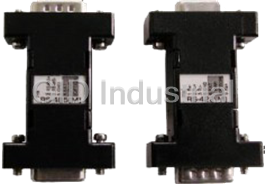
Self powered DB9 RS-232 to DB9 RS-422 Serial Data Converter
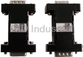
Self powered DB9 RS-232 to DB9 RS-485 Serial Data Converter
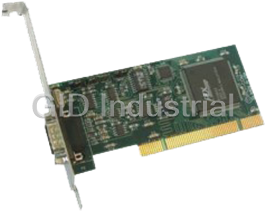
High-Speed, Low-Profile, Universal PCI, 16-bit Multifunction Analog I/O Board
Low Profile single port asynchronous serial communication card that can be installed in any 3.3V or ...

Low Profile Quad-port asynchronous RS-232serial communication card that can be installed in any 3.3V...
Request a Quote

The quote request has been received
Close

Facing challenges or have inquiries? Feel free to contact us!
Call Us +1-469-283-2440
What they say about us
FANTASTIC RESOURCE
One of our top priorities is maintaining our business with precision, and we are constantly looking for affiliates that can help us achieve our goal. With the aid of GID Industrial, our obsolete product management has never been more efficient. They have been a great resource to our company, and have quickly become a go-to supplier on our list!
Bucher Emhart Glass
EXCELLENT SERVICE
With our strict fundamentals and high expectations, we were surprised when we came across GID Industrial and their competitive pricing. When we approached them with our issue, they were incredibly confident in being able to provide us with a seamless solution at the best price for us. GID Industrial quickly understood our needs and provided us with excellent service, as well as fully tested product to ensure what we received would be the right fit for our company.
Fuji
HARD TO FIND A BETTER PROVIDER
Our company provides services to aid in the manufacture of technological products, such as semiconductors and flat panel displays, and often searching for distributors of obsolete product we require can waste time and money. Finding GID Industrial proved to be a great asset to our company, with cost effective solutions and superior knowledge on all of their materials, it’d be hard to find a better provider of obsolete or hard to find products.
Applied Materials
CONSISTENTLY DELIVERS QUALITY SOLUTIONS
Over the years, the equipment used in our company becomes discontinued, but they’re still of great use to us and our customers. Once these products are no longer available through the manufacturer, finding a reliable, quick supplier is a necessity, and luckily for us, GID Industrial has provided the most trustworthy, quality solutions to our obsolete component needs.
Nidec Vamco
TERRIFIC RESOURCE
This company has been a terrific help to us (I work for Trican Well Service) in sourcing the Micron Ram Memory we needed for our Siemens computers. Great service! And great pricing! I know when the product is shipping and when it will arrive, all the way through the ordering process.
Trican Well Service
GO TO SOURCE
When I can't find an obsolete part, I first call GID and they'll come up with my parts every time. Great customer service and follow up as well. Scott emails me from time to time to touch base and see if we're having trouble finding something.....which is often with our 25 yr old equipment.
ConAgra Foods