

 Manufacturers
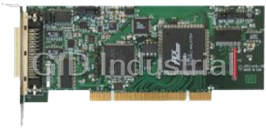
PORTWELL LPCI-A16-16A
Description
None available.
Part Number
LPCI-A16-16A
Price
Request Quote
Manufacturer
PORTWELL
Lead Time
Request Quote
Category
I/O Products
Specifications
Categorization Information
IO Products
Features
- Universal PCI, PCI-X, 3.3V and 5V compatible
- 16 Single-Ended / 8 Differential Analog Inputs
- 12-Bit Resolution, 100kHz A/D Converter
- Eight Programmable Voltage Ranges (Unipolar and Bipolar) and 4-20mA Current Range
- FIFO Data and Point List Buffers. Both FIFOs 2K Samples
- On-board Pacer Clock and Counter Timers
- Two 12 bit Analog Outputs
- 24 Buffered Digital I/O Lines
- Software Drivers Included for Windows 95/98/NT/2000/XP, and LabVIEW under Windows 95/98/NT
- * This product has been discontinued. * NEWS ! we has designed the replacement for this discontinued product. New product at LPCI-AIO16A
Datasheet

Extracted Text
Model LPCI-A16-16A 16-Bit Analog and Digital I/O Card USER MANUAL FILE: MLPCI-A16-16A.C1d Notice The information in this document is provided for reference only. Portwell does not assume any liability arising out of the application or use of the information or products described herein. This document may contain or reference information and products protected by copyrights or patents and does not convey any license under the patent rights of Portwell, nor the rights of others. IBM PC, PC/XT, and PC/AT are registered trademarks of the International Business Machines Corporation. Printed in USA. Copyright 2005 by Portwell I/O Products Inc, 44200 Christy Street, Fremont, CA 94538. All rights reserved. WARNING!! ALWAYS CONNECT AND DISCONNECT YOUR FIELD CABLING WITH THE COMPUTER POWER OFF. ALWAYS TURN COMPUTER POWER OFF BEFORE INSTALLING A CARD. CONNECTING AND DISCONNECTING CABLES, OR INSTALLING CARDS INTO A SYSTEM WITH THE COMPUTER OR FIELD POWER ON MAY CAUSE DAMAGE TO THE I/O CARD AND WILL VOID ALL WARRANTIES, IMPLIED OR EXPRESSED. 2 Manual LPCI-A16-16A Warranty Prior to shipment, Portwell equipment is thoroughly inspected and tested to applicable specifications. However, should equipment failure occur, Portwell assures its customers that prompt service and support will be available. All equipment originally manufactured by Portwell which is found to be defective will be repaired or replaced subject to the following considerations. Terms and Conditions If a unit is suspected of failure, contact Portwell' Customer Service department. Be prepared to give the unit model number, serial number, and a description of the failure symptom(s). We may suggest some simple tests to confirm the failure. We will assign a Return Material Authorization (RMA) number which must appear on the outer label of the return package. All units/components should be properly packed for handling and returned with freight prepaid to the Portwell designated Service Center, and will be returned to the customer's/user's site freight prepaid and invoiced. Coverage First Three Years: Returned unit/part will be repaired and/or replaced at Portwell option with no charge for labor or parts not excluded by warranty. Warranty commences with equipment shipment. Following Years: Throughout your equipment's lifetime, Portwell stands ready to provide on-site or in-plant service at reasonable rates similar to those of other manufacturers in the industry. Equipment Not Manufactured by Portwell Equipment provided but not manufactured by Portwell is warranted and will be repaired according to the terms and conditions of the respective equipment manufacturer's warranty. General Under this Warranty, liability of Portwell is limited to replacing, repairing or issuing credit (at Portwell discretion) for any products which are proved to be defective during the warranty period. In no case is Portwell liable for consequential or special damage arriving from use or misuse of our product. The customer is responsible for all charges caused by modifications or additions to Portwell equipment not approved in writing by Portwell or, if in Portwell opinion the equipment has been subjected to abnormal use. "Abnormal use" for purposes of this warranty is defined as any use to which the equipment is exposed other than that use specified or intended as evidenced by purchase or sales representation. Other than the above, no other warranty, expressed or implied, shall apply to any and all such equipment furnished or sold by Portwell. 3 Manual LPCI-A16-16A Table of Contents Chapter 1: Overview Functional Description............................................................................6 Figure 1-1: Block Diagram................................................................................................................................... 8 Chapter 2: Installation ................................................................................................................9 Chapter 3: Option Selection.....................................................................................................10 Figure 3-1: Option Selection Map...................................................................................................................... 10 Address and Interrupt Determination ................................................................................................................. 11 D/A Range Configuration................................................................................................................................. 11 A/D Configuration............................................................................................................................................. 11 Table 3-1 Range Selection................................................................................................................................. 11 Range/Mode Selection ..................................................................................................................................... 12 Loading A/D Calibration Constants................................................................................................................ 12 Chapter 4: A/D Converter Operation .......................................................................................13 Overview: A/D Operational Modes ...................................................................................................................... 13 Breakdown: A/D Operational Modes................................................................................................................... 14 Mode 1. Software:...................................................................................................................................... 14 Mode 2. Burst Mode:................................................................................................................................. 14 Mode 3. Timed: (Counter Triggered) ....................................................................................................... 14 Mode 4. External Start of Triggered (TIMED) Mode Above. .................................................................. 14 Mode 5. External Trigger Control. ........................................................................................................... 14 Step-By-Step: A/D Operational Modes ............................................................................................................... 15 Mode 1. Software Step-by-Step................................................................................................................ 15 Mode 2. Burst Mode Step-By-Step .......................................................................................................... 15 Mode 3. Triggered (TIMED) Step-By-Step............................................................................................... 16 READ DATA FAST ................................................................................................................................................ 17 Chapter 5: Digital Input/Output and Analog Output...............................................................18 Digital Input/Output .............................................................................................................................................. 18 Analog Output ....................................................................................................................................................... 18 Chapter 6: Programming..........................................................................................................19 8-Bit Address Map .............................................................................................................................................. 19 16-Bit Address Map ............................................................................................................................................ 20 8-Bit Register Definitions..................................................................................................................................... 21 8-Bit Base Address + 0 - Start A/D Conversion (Write) ................................................................................ 21 8-Bit Base Address + 1 - A/D Data FIFO Reset .............................................................................................. 21 8-Bit Base Address + 2 - A/D Channel Scan Control (Write only) ............................................................... 21 8-Bit Base Address + 3 - A/D Burst Mode Control (Write Only)................................................................... 21 8-Bit Base Address + 8 - Jumper Configuration / Status (Read) ................................................................. 22 8-Bit Base Address + 9 - Internal Status Register (Read) ........................................................................... 22 8-Bit Base Address + A - EEPROM Data Write and Read............................................................................. 22 Writing to the EEPROM ........................................................................................................................................ 23 Reading from the EEPROM.................................................................................................................................. 24 8-Bit Base Address + A - A/D Channel Read (Bits 3 - 0)............................................................................... 24 8-Bit Base Address + B - Calibration Data Write........................................................................................... 25 8-Bit Base Address + C - Interrupt Enable (Write Only) ............................................................................... 26 8-Bit Base Address + D - A/D Format Select (Write Only)............................................................................ 27 8-Bit Base Address + 10 - Digital I/O Bits 0 - 7 .............................................................................................. 27 8-Bit Base Address + 11 - Digital I/O Bits 8 - 15 ............................................................................................ 27 8-Bit Base Address + 14 through + 17 - Counter/Timer................................................................................ 27 8-Bit Base Address + 19 - Reset Digital I/O to Input Mode (Write) .............................................................. 27 8-Bit Base Address + 1A - Configure Oversampling (Write Only)............................................................... 27 8-Bit Base Address + 1B - A/D Counter Trigger Select (Write Only)........................................................... 28 8-Bit Base Address + 1C - EXTERNAL TRIGGER Selection (Write Only)................................................... 28 8-Bit Base Address + 1D - Board Reset (Read) ............................................................................................. 28 8-Bit Base Address + 1E - Enable Counters (Write Only)............................................................................ 28 16-Bit Register Definitions................................................................................................................................... 30 16-Bit Base Address + 0 - Read A/D Data FIFO (Word Read)....................................................................... 30 16-Bit Base Address + 4 - Software Gain Select 0-7 (Word Write) .............................................................. 30 4 Manual LPCI-A16-16A 16-Bit Base Address + 6 - Software Gain Select 8-15 (Word Write) ............................................................ 31 16-Bit Base Address + 8 - DAC 1 Output / DAC Control (Word Write) ........................................................ 31 16-Bit Base Address + E - DAC 0 Output / DAC Control (Word Write)........................................................ 31 Chapter 7: Connector Pin Assignments .................................................................................32 Appendix A: Technical Specifications ....................................................................................33 Appendix B: 82C54 Counter Timer Operation........................................................................35 OPERATIONAL MODES........................................................................................................................................ 35 Mode 0: Pulse on Terminal Count................................................................................................................... 35 Mode 1: Retriggerable One-Shot..................................................................................................................... 35 Mode 2: Rate Generator................................................................................................................................... 35 Mode 3: Square Wave Generator .................................................................................................................... 35 Mode 4: Software Triggered Strobe................................................................................................................ 35 Mode 5: Hardware Triggered Strobe .............................................................................................................. 36 PROGRAMMING.................................................................................................................................................... 36 READING AND LOADING THE COUNTERS ....................................................................................................... 37 Appendix C: Calibration ...........................................................................................................39 Overview: Calibrating without using the provided calibration program......................................................... 39 Breakdown: Calibrating the DACs ...................................................................................................................... 40 Step-By-Step: Calibrating the DACs ................................................................................................................... 41 Breakdown: Calibrating the A/D.......................................................................................................................... 42 Step-By-Step: Calibrating the A/D....................................................................................................................... 43 Table C-1: Factory EEPROM Calibration Locations.......................................................................................... 44 5 Manual LPCI-A16-16A Chapter 1: Overview Functional Description This card is a high-speed, high-resolution universal PCI data acquisition card. Designed for compatibility with both PCI and PCI-X bus slots as well as Low Profile Computers, the card is perfect for the instrumentation system designer. It is useful for precision measurement and control in applications such as standalone environmental test stations, compact production test equipment, portable testers, avionics and others. The card’s ability to trigger the A/D (Analog to Digital) in real time assures precisely timed sampling that is unaffected by other computer operations. This is an essential requirement for signal, vibration and transient analysis where high data rates must be sustained for short periods of time. This high-speed sampling rate is supported by a data FIFO for reducing processor overhead. Other functions engineered into this card are sixteen parallel bits of digital I/O, a 16-bit counter, and two analog outputs. The card is shipped with a suite of software drivers, samples and support in the most common programming languages. Analog Inputs 16 S.E. (Single-Ended) or 8 Diff. (Differential) 16-Bit resolution Analog Inputs are available and configured via a jumper on the card. Any single channel can be acquired at 500,000 samples / second, or any range of channels can be acquired at 450,000 samples / second. The high-impedance Analog Inputs feature hardware / software selectable ranges of 0-1V, 0-2V, 0-4V, 0-5V, 0-10V, ±0.5V, ±1V, ±2V, ±2.5V, ±5V, and ±10V. All the data from the A/D is placed directly into a 1K Sample FIFO (larger FIFOs available, contact factory) to enhance the maximum throughput of the card. The A/D can be operated in five different modes: software, burst mode, counter timed, external start of timed mode and external trigger control mode. Analog Outputs Two double-buffered 12-Bit Digital-to-Analog (D/A) converter outputs are provided. Output ranges of 0-5V and 0-10V are setup per channel with an on-board jumper. Digital I/O 16 Buffered Digital Input/Outputs are provided. Each TTL output can sink 24mA or source 15mA. All 16 lines may be programmed as inputs or outputs or 8 lines may be inputs while the other 8 are outputs. All lines are pulled up to 5 Volts via 10K ohm resistors. These resistors are very useful for reliably reading dry contact closures. Consult the factory to specify special resistor configurations. Counter/Timer The card contains an 82C54 Programmable Interval Timer (three sixteen bit counters). The counters are generally used to time the A/D conversion process, but two can also be used for frequency generation. Consult Chapter 4, Chapter 6, and Appendix B for more information on the A/D, programming, and the counter itself. Calibration This card features digitally controlled potentiometers to adjust the gain and offset of the A/D and the gain of the D/A. This allows both the analog inputs and outputs to be calibrated from software in the field. In order to obtain accurate data, the proper calibration values must be loaded into the digital potentiometers each time the card is powered. The factory calibrates each card’s inputs and outputs prior to shipment. These calibration values are stored in an on-board EEPROM allowing simple reuse of calibration data from one boot to the next. It is highly recommended to calibrate the card in the installed application environment for the most accurate results. For details refer to Chapter 6 on programming and Appendix C on Calibration. 6 Manual LPCI-A16-16A Software The card is supported for use in all operating systems and includes a free DOS, Linux and Windows 95/98/Me/NT/ 2000/XP compatible software package. This includes sample programs and source code in "C" and Pascal for DOS, and Visual Basic, Delphi, C++ Builder, and Visual C++ for Windows. Also included is a graphical setup program in Windows. Linux support includes installation files and basic samples for programming from user level via an open source kernel driver. I/O Connector and Accessories On the card’s mounting bracket is a 50-pin female type-II SCSI, I/O connector. All the card’s functions (A/D, D/A, DIO, CTR) are accessed via this connector. One-touch lock-latches are used as the cable retention mechanism. Optionally, a shielded 3 foot (1 Meter) round-wire molded cable assembly and screw-terminal board for convenient connection to an application are available. Refer to Chapter 7 for the pin assignments of the I/O connector. 7 Manual LPCI-A16-16A Figure 1-1: Block Diagram 8 Manual LPCI-A16-16A Chapter 2: Installation Configure Card Options via Jumper Selection Before installing the card into your computer, carefully read Chapter 3: Option Selection of this manual, then configure the card according to your requirements. Our Windows based setup program can be used in conjunction with Chapter 3 to assist in configuring jumpers on the card, as well as provide additional descriptions for usage of the various card options. The software provided with this card is contained on CD and must be installed onto your hard disk prior to use. CD Software Installation DOS/WIN3.x 1 Place the CD into your CD-ROM drive. 2 Change the active drive to the CD-ROM drive. 3 Run the install program (install.exe). 4 Follow the prompts to install the software for the LPCI-A16-16A WIN95/98/NT/2000/XP 1 Place the CD into your CD-ROM drive. 2 The install program should automatically run. If the install program does not run automatically, click START | RUN and type B GLQR?JJ, click OK or press ENTER. 3 Follow the prompts to install the software for the card. LINUX/UNIX and Other OS’s 1 Place the CD into your CD-ROM drive. 2 Follow the prompts to install the software for the card. Leave the Portwell Master CD in the drive and proceed to the next step. Installing the Card into the Computer slot CAUTION! * / ESD A single static discharge can damage your card and cause premature failure! Please follow all reasonable precautions to prevent a static discharge such as grounding yourself by touching any grounded surface. 1 If the computer is a Low-Profile Computer then back out the two screws on the I/O connector to remove the regular size bracket that ships installed on the card, and install the Low-Profile bracket onto the card and tighten the connector’s bracket screws. (Save the regular size bracket in case the card ever needs to be moved to another computer at a later time.) 2 Shut down the computer and remove the cover. 3 Install the card in the computer paying particular attention to the mounting bracket’s retention screw to ensure a good ground connection exists. 4 Install an I/O cable onto the card’s I/O connector. 5 Power on the computer, which should auto-detect the card (depending on operating system) and automatically finish installing the drivers. 6 Run PCIfind.exe to complete installing the card into the registry and to determine the assigned resources. 7 Now would be a good time to run one of the provided sample programs that was copied to the newly created card directory from the CD to test and validate your installation. 9 Manual LPCI-A16-16A Chapter 3: Option Selection Jumpers are available on the card to setup the following selections: A/D input mode (S.E. or Diff.) A/D range (Hi Gain / Lo Gain)D/A output voltage ranges The Setup Program from the Software Master CD may be referred to for assistance in selecting the appropriate options for your application. Software can determine the jumper selections by reading the status register at 8-Bit Base Address + 8 (Chapter 6). The standard card has a Counter/Timer, two 12-bit Analog Outputs, 16 lines of Digital I/O, and a 16 channel, 16-bit 500Khz A/D Converter with 1K Sample FIFO. GNHi 0-10V S.E. GNLo 0-5V DIFF BIPOLAR UNIPOLAR DAC 0 DAC 1 Figure 3-1: Option Selection Map 10 Manual LPCI-A16-16A Address and Interrupt Determination The Card’s base addresses and interrupt are automatically selected by your computer. The utility PCIFind.exe may be used to determine the addresses and interrupt chosen by the computer. *Note that if the card is moved to a different slot, or other hardware is added or removed, the computer may select different addresses and/or interrupts for previously installed cards. D/A Range Configuration This card provides two independent analog outputs. Each analog output is adjusted by output calibration circuitry including a digital potentiometer. The digital calibration potentiometers are serial devices, with data being automatically loaded bit by bit at boot-time, or during active calibration. Although the details of writing bit by bit are described in Chapter 6, it is expected that data will be loaded by using the supplied software subroutines. In order to obtain accurate analog output voltages, the following operations must be performed: 1) The desired output ranges (0-5 and 0-10V) must be selected by means of jumper selections on the card. The Option Selection Map and Setup Program provide convenient references for setting these options. There are two jumpers, labeled DAC 0 and DAC 1, respectively. To select the range for channel 0, a jumper needs to be installed at DAC 0. To select the 5 Volt range, the jumper should be in the position nearer the I/O connector. To select the 10 Volt range, the jumper should be in the position away from the I/O connector. To select the range for channel 1, a jumper needs to be similarly installed at DAC 1. 2) The correct calibration constants must be loaded into the digital potentiometers that adjust the output circuitry. The card is calibrated prior to shipment but it is highly recommended that field calibration be done prior to system commissioning. (This operation is described in Appendix C: Calibration). A/D Configuration In order to use the A/D properly, the following operations must be completed: 1) The range of the A/D must be set by selecting jumpers on the board. See the Option Selection Map or card setup program for the positions of these jumpers. 2) The mode (S.E. or DIFF.) of the A/D input must be chosen by selecting jumpers on the board. 3) The appropriate calibration constants should be loaded into the digital calibration potentiometers used with the A/D. Prog Gain=0 Prog Gain=3 Jumpers Prog Gain=1 (x2) Prog Gain=2 (x5) (x1) (x10) Unipolar 0 - 10V 0 - 5V 0 - 2V 0 - 1V GNH Bipolar ± 5V ± 2.5V ± 1V ± 0.5 Unipolar invalid 0 - 10V 0 - 4V 0 - 2V GNL Bipolar ± 10V ± 5V ± 2V ± 1V Table 3-1 Range Selection 11 Manual LPCI-A16-16A Range/Mode Selection Carefully plan which range to select on the card by examining Table 3-1. Only the ranges shown in a single row are available simultaneously (via software control). For example, if you want to use both ±5V and ±2V inputs, you must select GNL/Bipolar range; if you’re using only ±5V inputs you could select either GNH/Bipolar or GNL/Bipolar (although GNH/Bipolar would be simpler from a software perspective, as the programmable gain defaults to “0", the correct value for this range.) These jumper settings are shown on the Option Selection Map. 1) The maximum span of the A/D circuitry is selected by choosing the GNH (high gain) or GNL (low gain) jumpers, located at the top edge of the card. Note that there are two side-by-side jumpers that must be installed in pairs, one below the other. One jumper makes the makes the Analog gain connection, while the other “tattletale jumper” informs the Digital PLD, Programmable Logic Device, of the selection. This information allows Software to understand and properly display the data read from the FIFO. Another pair of jumpers must be installed to determine whether the ranges are unipolar (i.e. 0-10V) or bipolar (i.e. +/- 5V). These jumpers are located beside the gain jumpers at the top edge of the card. These should also be installed in pairs. One jumper is an Analog selection jumper while the other is a “tattletale” jumper. 2) The Diff/SE mode of the multiplexer and the A/D circuitry is selected by installing two jumpers. One is an Analog jumper selection while the other is a Digital “tattletale” jumper. These two jumpers determine the Mode of the input multiplexers 16 CH SE, 16 channels single ended, jumpers in topmost position or 8 CH BAL, 8 channels balanced (differential), jumpers installed in bottommost position. Select the mode of the multiplexer to either 8 channels of differential inputs (results in measuring the difference between 2 points without reference to ground), or 16 channels of single ended inputs (measured between a single wire and a ground common to all the other analog inputs). ***Combinations of both SE and DIFF inputs are not supported for use by this card, with the exception that it is possible to read a SE input with a differential channel. The programmable gain amplifier may also be set through software. If not programmed, the default gain is x1 (gain code 0). Loading A/D Calibration Constants The gain and offset of the signal conditioning circuitry are adjusted by means of digital potentiometers. If constants are not loaded, the potentiometers will be set to the center of their ranges, by default. Therefore, for maximum accuracy on each channel, appropriate settings should be entered into them each time the board is powered. Consult Appendix C: Calibration for information on how to determine and load appropriate settings. 12 Manual LPCI-A16-16A Chapter 4: A/D Converter Operation The A/D circuitry on this card forms a very powerful and flexible framework on which you can build a broad array of data acquisition applications. The rest of this chapter is broken down into several sections. The first section is an Overview, which will introduce you to the three most common modes of using the A/D. This will be followed by a Breakdown of the steps recommended to use each of the three modes. Next, a Step-By-Step walkthrough is provided. Steps are numbered consistently between the three sections so you can easily flip between them to build an understanding of the process. Following these discussions of the A/D operational modes is some explanation of the various methods of reading the A/D data from the card. Before using any Analog function of the card, make sure you’ve configured the jumpers as described in Chapter 3. Also, make sure the proper calibration constants have been loaded into the calibration potentiometers using the procedures discussed in Appendix C, as shown in the sample programs. Except in burst mode, the card selects channels via “scans”. A scan includes the starting and ending channels, plus all channels in between. For example, a scan from channels 2 to 5 would be 2, 3, 4, and 5, for a total of four samples per scan. A software mode start command starts one sample, while a triggered mode trigger starts an entire scan. In contrast, Burst Mode will only aquire data from a single channel, the first channel specified in the scan control register. Overview: A/D Operational Modes Five modes of A/D operation are available: Mode 1. Software: Write to 8-bit base + 0. Takes one entry from the 8-bit base + 2 scan register and increments the channel. This mode is very simple and straightforward, but requires much of the CPU’s attention and is limited in speed. Mode 2. Burst Mode: Takes data at 2:sec/conversion (500KHz) on a single channel. Mode 3. Timed: (Counter Triggered) Takes one scan of data at a very fast rate each time the configured counter times out. Each entry in the scan is taken “oversample” number of times. **Note “oversample” may be 1, 2, 8, or 16 times on the same channel. Mode 4. External Start of Timed Mode (above). Once A/D acquisition has begun, this Mode performs exactly as Mode 3. However, an External Trigger is required to initiate the first SCAN. Mode 5. External Trigger Control Mode. After setup software programming, an A/D data SCAN occurs for each rising edge of the External Trigger. 13 Manual LPCI-A16-16A Breakdown: A/D Operational Modes The following describes the five modes of operation in more detail. Please note: in the following sections the nomenclature (+xx) indicates “performed at the register available at Base address of the card +offset xx, or the register xx. Mode 1. Software: 1.0 Reset Board (+1D). Read +1D, Ignore returned data. 1.1 Set Channel Scan Limits (+ 2). Write Start Channel (lower nybble) + Stop Channel (upper nybble). Note: one combined 8bit Write. 1.2 Set Gain Codes (+4) for A/D input channels 0 through 7. Set Gain Codes (+6) for A/D input channels 8 through 15(F) hex. 1.3 Loop 1.31 Start Conversion (+0). Write any number to (+0). 1.32 Wait for FIFO not empty (+8) 1.33 Read Data (+0) 1.4 Until done Mode 2. Burst Mode: 2.1 Reset Board (+1D). Read +1D, Ignore returned data. 2.2 Set Channel (+ 2). See 1.1 above for details. 2.3 Set Gain Code (+4). See 1.2 above for details. 2.4 Start Burst (+3). Write 01 to (+3). 2.5 READ DATA FAST * 2.6 Disable Burst (+3). Write 00 to (+3) Mode 3. Timed: (Counter Triggered) 3.1 Reset Board (+1D). Read +1D, Ignore returned data. 3.2 Set Channel Scan Limits (+ 2). See 1.1 above. 3.3 Set Gain Codes (+4). See 1.2 above. 3.4 Configure Counters (below). 3.5 Enable Counters (+1E), write 40. 3.6 Configure Oversampling And Enable Timed A/D (+1A), write 11 for NO Oversampling. Write 91 for 2 samples of each channel selected. Write 90 for 8 samples, or write 10 for 16 samples for a selected channel before the next channel is selected. 3.7 Start A/D conversions by writing (+1B). Write 01 (use counters 1+2, or write 03, (use counter 0 only). 3.8 READ DATA FAST * 3.9 Reset Board (+1D) to stop A/D conversions, Read +1D. Mode 4. External Start of Triggered (TIMED) Mode Above. This is the same as Mode 3, except Step 3.7 does not start conversions. 4.1 Connect an external trigger to pin 36 of Connector P3 (I/O connector on the card mounting bracket), connect trigger return lead to Ground at the card. The trigger State may be either high or low at this time, but MUST NOT be changing state. 4.2 to 4.6, use instructions 3.1 through 3.6 above. 4.7 Same as 3.7 above EXCEPT, (+1B) Write 00 (use counters 1+2), or write 02 (use counter 0 only). 4.8 Start A/D conversions by allowing a rising edge trigger to occur. Only the FIRST trigger is used to START the A/D conversion sequence. A/D scans will continue until stopped. 4.9 READ DATA FAST *. Mode 5. External Trigger Control. Or One Scan Per Trigger Mode. This mode allows full external control of the RATE at which A/D scans occur. A SCAN may consist of converting 1 to 16 channels of analog input data. The number of A/D conversions per scan consists of the number of input channels selected multiplied by the number of oversamples (usually only one sample per channel). 5.1 Connect an External Trigger to pin 35 of Connector P3. The trigger State may be high or low at this time but should not be changing state (running) until the Software Program is ready for A/D acquisition. 14 Manual LPCI-A16-16A 5.2 Reset Board (+1D), Read +1D, ignore returned data. 5.3 Set Channel Scan Limits. See step 1.1 above. 5.4 Set A/D gain Codes (+4). See step 1.2 above. 5.5 Pre-Enable External Trigger Control (+1C). Write 02 to (+1C). 5.6 The Card is now ready to start acquiring A/D data which it will do when the next rising edge of the external trigger occurs. 5.7 The Software Program will now acquire one A/D SCAN for each external trigger. No new data will be taken until the next external trigger occurs. 5.8 READ DATA FAST*. 5.9 The program may be halted temporarily by writing 00 to (+1C). The Program will resume by writing 02 to (+1C). 5.10 To clear the program completely, read data from (+1D). * Several methods exist to read the data quickly from the card. Consult the section READ DATA FAST at the end of this chapter. Step-By-Step: A/D Operational Modes Now lets describe these modes in detail. All Base + xx offsets are in hexadecimal. Please refer to Chapter 6: Programming for more information on these registers. Mode 1. Software Step-by-Step Step 1.0 Reset Board (+1D), Read +1D, ignore returned data. Step 1.1 Set Channel Scan Limits. 8-Bit Base + 2 contains the Start and End Channel Scan Limit register. The top nybble is the End Channel, the bottom nybble is the Start Channel. In this mode the A/D will take its first conversion on the Start channel. The channel number then increments until it is larger than the End Channel entry, and starts over at the Start Channel. The current channel can be read at 8-Bit Base + A, should the need arise. Any time you write to this register the current channel is set to the Start Channel. Step 1.2 Set Gain Codes. This optional step allows you to configure a different gain code per channel, allowing for different input ranges on each channel of the card. To set the gain codes, write to 16- Bit Base + 4 and 16-Bit Base + 6. Refer to Table 3-1 in Chapter 3 for a quick range/gain reference. Note: All channels are initially set for a gain of one, and can be reset by writing to (+7) Step 1.3 Loop. In step 1.4 you’ll come back to this step. Step 1.31 Start Conversion. Writing any value to 8-Bit Base + 0 will start a conversion on the current channel. When the conversion is completed the data will be moved into the A/D Data FIFO, and the EMPTY bit in 8-Bit Base + 8 will indicate the presence of data in the FIFO. Step 1.32 Wait for FIFO not empty. By checking the EMPTY bit in 8-Bit Base + 8 determine when the FIFO has received the A/D data. W hile you are waiting your program can perform other operations, such as DAC outputs, without disturbing the A/D. Step 1.33 Read Data. Read from 16-Bit Base + 0 to retrieve the results of the conversion from the A/D Data FIFO. Once you have the data you can store it on disk, display on screen, or whatever else your system requires. Step 1.4 Until Done. Repeat from 1.3 until you don’t need any more data. Mode 2. Burst Mode Step-By-Step Step 2.1 Reset Board (+1D), Read +1D, ignore returned data. Step 2.2 Set Channel. Burst mode only takes data from one channel. Write the channel you want to take data from to 8-Bit Base + 2. Only the bottom nybble is significant. Step 2.3 Set Gain Code. All of the data taken will be at the same gain code / range. Specify the range you want by writing to 16-Bit Base + 4 or + 6. Refer to Table 3-1 in Chapter 3 for a quick range/gain reference. Step 2.4 Start Burst. Write “1" to 8-Bit Base + 3 to enable Burst Mode. As each conversion completes the data will be moved into the A/D Data FIFO. If any data is in the FIFO the EMPTY bit will so indicate, and if the FIFO reaches half-full, the DFH bit will so indicate (8-Bit Base + 8). Step 2.5 READ DATA FAST. The maximum rate, 500KHz, is fast. If you fail to take the data out of the FIFO fast enough, it will fill. If the FIFO reaches full, the burst will pause until some data has been removed from the FIFO to make room for more. Various methods for reading the data are explained in the section READ DATA FAST, below. 15 Manual LPCI-A16-16A Step 2.6 Disable Burst. Whenever you have enough data for your needs, write “0" to 8-Bit Base + 3 to stop the A/D conversions. Mode 3. Triggered (TIMED) Step-By-Step Step 3.1 Reset Board(+1D), Read +1D, ignore returned data. Step 3.2 Set Channel Scan Limits. Please see Step 1.1, above, for information. Step 3.3 Set Gain Codes. Please see Step 1.2, above, for information. Step 3.4 Configure Counters. Place Counters 1+2 in Mode 2, with a load value appropriate to the timing you want. The input frequency to Counter 1 is 10MHz, the input to Counter 2 is the output of Counter 1. Therefore, the equation to determine the needed load value for the “32bit” Counter 1+2 is 10,000,000/RateInHertz. For example, if you want scans to start every 15 milliseconds, your equation is 10,000,000 / (1 / (0.015)) = 10,000,000/ 66.67 = 150,000. This load value must then be allocated to the two 16-bit counters which make up the 32-bit Counter 1+2. If the counters accepted fractional load values, the simplest method would be to take the square-root of 150,000. Instead, find two integer factors of 150,000 each smaller than 65,535 and larger than 1. 3 and 50,000 work fine; load Counter 1 with 3 and Counter 2 with 50,000, and your scan rate is set at 66.67Hz. It is important that the ScanStart trigger does not occur during a scan. When using the counter(s) you must have a long enough timeout period loaded in Counters 1+2 that the card has time to complete "Oversample" number of conversions on as many channels as you have selected at 8-Bit Base + 2. I.e., if you are acquiring 8 channels of data, you need at least (8*2.2µSec=17.6) 17.6 microseconds between scan starts. See Appendix B for more information on loading the counters. Step 3.5 Enable Counters. By writing “40" to 8-Bit Base + 1E you Preenable the gates of Counters 1+2, and by writing “01" to 8-Bit Base + 1B you enable scans started by Counters 1+2. Once Step 3.6 is performed and the counters have timed out a scan will start. Step 3.6 Configure Oversampling And Enable Timed A/D. In this mode of operation the A/D is capable of taking more data than your application will eventually want, very efficiently. The resultant data can be averaged in software to provide very-low-noise digital data. 1x, 2x, 8x, or 16x the data per channel can be acquired. Each channel is acquired multiple times before the channel number is incremented, causing the data to have very little skew in time. Write to 8-Bit Base + 1A to configure the Oversample feature and enable acquisition. Step 3.7 READ DATA FAST. See Step 2.6 and below for more information. 16 Manual LPCI-A16-16A READ DATA FAST The card contains a 2048-byte A/D Data FIFO configured as a 1024-sample FIFO. The FIFO provides two status bits useful when taking data from the card. First, a Data FIFO Half (DFH) bit is available. This bit indicates the FIFO is now half full. In addition this bit, if enabled, will generate an IRQ. Second, an EMPTY bit is provided which indicates the FIFO contains no data; if there is any data in the FIFO, the EMPTY bit will not be true. Using combinations of these two bits and the DFH IRQ allows several fast and efficient methods of taking the data from the FIFO. Perhaps the simplest method of taking data is to read one sample at a time using a read of 16-Bit Base + 0. In this mode, you determine when to read the sample by polling the EMPTY bit. When the FIFO is not empty, you read one sample. This method is simple to program, but not very resource efficient; reading the status register and the FIFO for every sample can result in a very busy computer. Despite the drawbacks, this method is often the best when data rates are very slow, or the only goal is to quickly test operation of the card. The fastest method is INSW 512 samples from 16-Bit Base + 0 every time the DFH bit indicates the FIFO is half-full. Barely slower is to enable the IRQ to generate an IRQ each time DFH is true, and have an ISR respond to the IRQ by using INSW to read 512 samples. When the FIFO is filled, data acquisition pauses. It resumes when data is read from the FIFO, thereby changing its FULL state. 17 Manual LPCI-A16-16A Chapter 5: Digital Input/Output and Analog Output The use of the Digital Input/Output and Analog Output functions are completely controlled by application software and are described in more detail in Chapter 6: Programming. Digital Input/Output There are two independent Digital I/O ports. Each port consists of 8 bits. The external connections are made via the mounting bracket 50 pin SCSI connector and are listed in Chapter 7. Since each line is pulled up to +5V by 10Kohm resistors, the bits will read hi (0) with nothing connected externally. There are four (4) digital ground lines provided for connections related to signals that correspond to digital I/O lines and counter timer I/O lines. To monitor contact closures from relays, switches, etc., simply connect the switch from the I/O line to a nearby ground pin. When the contact closes, the line will drop to a low (0) which should be polled for in your application software at programmed time intervals. Port 0 is located at 8-Bit Base Address + 10 and reads/controls pins DIO0 through DIO7. Port 1 is located at 8-Bit Base Address + 11 and reads/controls pins DIO8 through DIO15. Both ports default to input (read) mode. Each remains in that mode until written to. When written to, that port will switch to and remain in output (write) mode. Both ports may be reset to the input mode by writing anything to 8-Bit Base Address + 19. Analog Output The DACs are controlled via two registers. Writing 0 to one of these registers results in 0V on the corresponding DAC, writing FFF results in either 5V or 10V according to the DAC’s jumper configuration. Writing AAA results in half of full scale, as the output values are linear through the full output range. The top 4 bits should be left zero when writing a value as these are 12-bit Digital to Analog Converters. The DAC mode is also controlled by writes to either of these registers. The card powers on in Automatic mode, in which each DAC changes to the value written as soon as you write it. The output’s beginning (default) value at power on is zero to prevent unwanted control outputs that may be connected to live equipment. Please refer to the appropriate section of Chapter 6 for more information. 18 Manual LPCI-A16-16A Chapter 6: Programming This card uses two address ranges, one for 16-Bit I/O and one for 8-Bit I/O. Both base addresses will be shown by PCIFind. The following tables show the register definition maps. All offsets are in hexadecimal. 8-Bit Address Map Offset Write Function Read Function 0 Start A/D Conversion 1 A/D Data FIFO Reset 2 A/D Channel Scan Control 3 A/D Burst Mode Control 4 5 6 7 8 Jumper Configuration / Status 9 Internal Status A EEPROM Data W rite EEPROM Read / A/D Channel Status B Calibration Data W rite C Enable IRQ D A/D Format Select E F 10 Digital Outputs 0 - 7 Digital I/O 0 - 7 11 Digital Outputs 8 - 15 Digital I/O 8 - 15 12 Software Configuration/ Status 13 14 Program Counter 0 Read Counter 0 15 Program Counter 1 Read Counter 1 16 Program Counter 2 Read Counter 2 17 Counter Control Register n/a 18 19 Reset Digital I/O to Input Mode 1A Oversampling, Enable ADC 1B A/D Counter Trigger Select 1C External A/D Trigger Select 1D Reset Board 1E Enable A/D Counters 1F 19 Manual LPCI-A16-16A 16-Bit Address Map Offset Write Function Read Function 0 Read A/D Data FIFO 2 4 A/D Software Gain Select 0-7 6 A/D Software Gain Select 8-15 7 Reset both Software gains to ONE 8 DAC 0 Output A E DAC 1 Output 10 12 14 16 18 1A 1C 1E Addresses left blank in the tables above are reserved for factory use, and should not be accessed by user software programs. 20 Manual LPCI-A16-16A 8-Bit Register Definitions 8-Bit Base Address + 0 - Start A/D Conversion (Write) Writing any value to this address causes the A/D to make one data acquisition and load it into the FIFO. This is known as a “Software Start Conversion” command. The channel acquired is the currently selected one in the A/D Channel Scan Control register. Please refer to the discussion in 8-Bit Base + 2 for information on selecting the channels. The channel advances after acqusition. 8-Bit Base Address + 1 - A/D Data FIFO Reset Writing any value to this address resets the FIFO. This will empty the FIFO of any data that remains. It is a good idea to reset the data FIFO before you start any data acquisition process to ensure you’re in good sync with the data that will be acquired. To make sure the FIFO reset will leave the FIFO empty, make sure the A/D isn’t currently acquiring data before issuing this command. Chapter 4 and the descriptions of 8-Bit Base Address + 3, + 1C, + 1D, and + 1E have more information on various ways acquisition could be happening. 8-Bit Base Address + 2 - A/D Channel Scan Control (Write only) Bit 7 Bit 6 Bit 5 Bit 4 Bit 3 Bit 2 Bit 1 Bit 0 EMA3* EMA2 EMA1 EMA0 SMA3* SMA2 SMA1 SMA0 This register controls the channel scan limits for the A/D input multiplexer. Specify a channel number from0 to 15 (0-F) in each nybble for the start and end limit of the auto-incrementing mux channel number. The “S” entries refer to the starting address for the scan and the “E” entries refer to the ending address for the scan. The scan is performed from the starting to the ending addresses, inclusively. No channels are omitted. Write same address in both nybbles to dwell on one channel. When the board is operated in the Differential mode, (E/S)MA3 is ignored. When the board is operated in the Single Ended mode, (E/S)MA3 is the most significant bit of the inputaddress. Notes: The selection of Single ended or Differential inputs must be made by properly installing jumpers on the card.Please refer to Chapter 3, or the Setup program, for details. Since the MUX addresses do not advance during the burst mode, the ending address (EMA3-EMA0) isignored, and all conversions occur on the channel specified in SMA3-SMA0. 8-Bit Base Address + 3 - A/D Burst Mode Control (Write Only) This register enables burst mode. Write 01 to start. Set desired channel using 8-Bit Base Address + 2 above. Burst Mode operation acquires data on one previously selected channel at the maximum speed of the A/D, approximately 2 microseconds per conversion (500KHz). This data is stored in the FIFO. Conversions pause when the FIFO is full. Conversions resume when a FIFO read command removes data from the FIFO (16-Bit Base + 0), thereby removing the FIFO full state. Alternatively, operation can be stopped short of a full FIFO if a Burst Mode Off command is sent (write 00 here). Usually you’ll be using the FIFO Half-full IRQ or polling its status bit to time when to take data out of the FIFO, ensuring it never reaches full. See 8-Bit Base Address + 8 for more information. 21 Manual LPCI-A16-16A 8-Bit Base Address + 8 - Jumper Configuration / Status (Read) Bit 7 Bit 6 Bit 5 Bit 4 Bit 3 Bit 2 Bit 1 Bit 0 EMPTY FULL DFH DA5V DB5V GNH BIPOLAR 16SE Bits 5, 6 and 7 provide status information about the card. EMPTY This bit is “1" when the A/D Data FIFO is empty. FULL This bit is “1" when the A/D Data FIFO is full. DFH This bit is “1" when the A/D Data FIFO contains more than half its capacity in data. This will also generate an IRQ if so enabled at 8-Bit Base + C. Bits 0, 1, 2, 3, and 4 are used for informing the software of the currently selected state of the Option Selection jumpers. Using this information enables the software to act in an almost plug-n-play fashion supporting all possible range and configuration options transparently. DA5V equals “1" when the DAC Channel A 5 Volt output range has been chosen by jumper selection. DB5V equals “1" when the DAC Channel B 5 Volt output range has been chosen by jumper selection. GNH equals “1" when the GNH jumper has been installed during option selection. BIPOLAR equals “1" when the bipolar/unipolar jumper is in the Bipolar position 16SE equals “1" when the 16-channel, single-ended A/D mode has been chosen by jumper selection. 8-Bit Base Address + 9 - Internal Status Register (Read) Bit 7 Bit 6 Bit 5 Bit 4 Bit 3 Bit 2 Bit 1 Bit 0 Read IRQEN GR1 GR0 F4 J1 F5 MRE MFF This register contains two bits useful when debugging programs that use the card; the remaining bits provideinternal diagnostic data, not needed for operational use. MFF is high if the FIFO is full, or if it has been full since this register was last read. MRE is high if a data read occurred without data in the FIFO since this register was last read. 8-Bit Base Address + A - EEPROM Data Write and Read Bit 7 Bit 6 Bit 5 Bit 4 Bit 3 Bit 2 Bit 1 Bit 0 Write Data X X X X X X SClock Read Data The EEPROM is intended to hold calibration data for the A/D Gain and Offset correction, and the Gain Correction data for both DACs. Calibration is only needed for GNL/GNH and BIP/UNI jumper selected ranges, so a total of 4 A/D Input calibration data pairs are used. Consult the provided calibration program or sample code for information on the locations in the EEPROM used to store the calibration data. Although the EEPROM is intended to contain calibration data, it is unlikely your program will need to keep calibration data for the ranges you are not going to use. In this case you can use those locations in the EEPROM for your own purposes. The Software Master CD contains sample programs demonstrating the use of the EEPROM in a variety of languages, including a “driverlet” which encapsulates the complexities of the process. Using this “driverlet” is as simple as passing the address and data in the EEPROM you wish to write, or the address from which to read, to our functions. It is highly recommended that you use the provided source code as a basis for your own programs. The following information is provided for portability only. 22 Manual LPCI-A16-16A Writing to the EEPROM Writing to the EEPROM is a three step process. First a write enable (EWREN) must be sent, the data transmitted and, then, a write disable (EWDS) sent. If several entries are to be made, only one write enable is required. Once the data is all entered, one write disable must be performed in order to protect the data in the EEPROM from inadvertent entries. Please note, it is not possible to write to the EEPROM until an EW REN sequence has been written to 8-Bit Base + A. The EWREN sequence consists of the following bytes, in order: 81, 01, 01, 81, 81, 01, 01, 01, 01, 00. Once the EW REN sequence has been written it is possible to write to the EEPROM as desired. In order to write data to the EEPROM, a start bit must be transmitted, then the Write opcode (2 bits, 01) followed by the address location of the data to be loaded into the EEPROM (6 bits, MSB first), followed by the data (16bits, MSB first). Then the transmission is ended with 0. Therefore, to write a value of aa55 to location 5, you would perform the following 26 writes: Write Value Description 1 1xxxxxx1 = 81 Start Bit. Always write 81 as the 1st byte 2 0xxxxxx1 = 01 opcode bit 1, always write 01 as 2nd byte for EEPROM writing 3 1xxxxxx1 = 81 opcode bit 0, always write 81 as 3rd byte for EEPROM writing 4 0xxxxxx1 = 01 MSB of address. Bit 7 should be 1 or 0 based on the D5 bit of address to be written. Always set D0 to “1" 5 Bit 7 should be bit D4 of address. Always set D0 to “1" 0xxxxxx1 = 01 6 Bit 7 should be bit D3 of address. Always set D0 to “1" 0xxxxxx1 = 01 7 Bit 7 should be bit D2 of address. Always set D0 to “1" 1xxxxxx1 = 81 8 Bit 7 should be bit D1 of address. Always set D0 to “1" 0xxxxxx1 = 01 9 1xxxxxx1 = 81 LSB of address. Bit 7 should be 1 or 0 based on the D0 bit of address to be written. Always set D0 to “1" 10 1xxxxxx1 = 81 MSB of data. Bit 7 should be 1 or 0 based on the D15 bit of address to be written. Always set D0 to “1" 11 Bit 7 should be bit D14 of data. Alwways set D0 to “1" 0xxxxxx1 = 01 12 Bit 7 should be bit D13 of data. Always set D0 to “1" 1xxxxxx1 = 81 13 Bit 7 should be bit D12 of data. Always set D0 to “1" 0xxxxxx1 = 01 14 Bit 7 should be bit D11 of data. Always set D0 to “1" 1xxxxxx1 = 81 15 Bit 7 should be bit D10 of data. Always set D0 to “1" 0xxxxxx1 = 01 16 Bit 7 should be bit D9 of data. Always set D0 to “1" 1xxxxxx1 = 81 17 Bit 7 should be bit D8 of data. Always set D0 to “1" 0xxxxxx1 = 01 18 Bit 7 should be bit D7 of data. Always set D0 to “1" 0xxxxxx1 = 01 19 Bit 7 should be bit D6 of data. Always set D0 to “1" 1xxxxxx1 = 81 20 Bit 7 should be bit D5 of data. Always set D0 to “1" 0xxxxxx1 = 01 21 Bit 7 should be bit D4 of data. Always set D0 to “1" 1xxxxxx1 = 81 22 Bit 7 should be bit D3 of data. Always set D0 to “1" 0xxxxxx1 = 01 23 Bit 7 should be bit D2 of data. Always set D0 to “1" 1xxxxxx1 = 81 24 Bit 7 should be bit D1 of data. Always set D0 to “1" 0xxxxxx1 = 01 25 1xxxxxx1 = 81 LSB of data. Bit 7 should be 1 or 0 based on the D0 bit of data written. Always set D0 to “1" 26 0xxxxxx0 = 00 End. Always write 00 as the 26th byte For ease of reference the bits which can change are typeset in bold. Once data entry is complete you you should disable writes to the EEPROM. A disable sequence of bytes may be written to 8-Bit Base + A as follows: 81, 01, 01, 01, 01, 01, 01, 01, 01, 00. 23 Manual LPCI-A16-16A Reading from the EEPROM Similarly, reading a word takes 10 writes (start bit, read opcode (2 bits 1,0) and the address (6 bits, MSB first)), followed by 16 reads to acquire the data from the eeprom, followed by one write to terminate communication with the eeprom. Therefore, to read from address 4, the following reads and writes are performed: Write Value Description 1 1xxxxxx1 = 81 Start Bit. Always write 81 as the 1st byte. 2 1xxxxxx1 = 81 Opcode Bit 1. Always write 81 as the 2nd byte for reading 3 0xxxxxx1 = 01 Opcode Bit 0. Always write 01 as the 3rd byte for reading 4 0xxxxxx1 = 01 MSB of address. Bit 7 should be 1 or 0 based on the D5 bit of address in the EEPROM to be Read. Always set D0 to “1" 5 Bit 7 should be bit D4 of address. Always set D0 to “1" 0xxxxxx1 = 01 6 Bit 7 should be bit D3 of address. Always set D0 to “1" 0xxxxxx1 = 01 7 Bit 7 should be bit D2 of address. Always set D0 to “1" 1xxxxxx1 = 81 8 Bit 7 should be bit D1 of address. Always set D0 to “1" 0xxxxxx1 = 01 9 0xxxxxx1 = 01 LSB of address. Bit 7 should be 1 or 0 based on the D0 bit of address to be read. Always set D0 to “1" Read 1 Bit D7 of this Read returns the Most Significant Bit (D15) of the 16-bit data stored at the address specified in writes 4 through 9. Read 2 D7 contains bit D14 from the word at the specified address Read 3 D7 contains bit D13 from the word at the specified address Read 4 D7 contains bit D12 from the word at the specified address Read 5 D7 contains bit D11 from the word at the specified address Read 6 D7 contains bit D10 from the word at the specified address Read 7 D7 contains bit D9 from the word at the specified address Read 8 D7 contains bit D8 from the word at the specified address Read 9 D7 contains bit D7 from the word at the specified address Read 10 D7 contains bit D6 from the word at the specified address Read 11 D7 contains bit D5 from the word at the specified address Read 12 D7 contains bit D4 from the word at the specified address Read 13 D7 contains bit D3 from the word at the specified address Read 14 D7 contains bit D2 from the word at the specified address Read 15 D7 contains bit D1 from the word at the specified address Read 16 D7 contains bit D0 from the word at the specified address Write 0xxxxxx0 = 00 End. Always Write 00 as the last step For ease of reference the bits which can change are typeset in bold. 8-Bit Base Address + A - A/D Channel Read (Bits 3 - 0) Bit 7 Bit 6 Bit 5 Bit 4 Bit 3 Bit 2 Bit 1 Bit 0 Read UNDER X F5 MA3* MA2 MA1 MA0 Bits 3 through 0 readback the currently in-use channel on the card. In auto-incrementing mux modes this data can be used to confirm proper operation of the device. MA3* In Single Ended Mode, this is the most significant bit of the A/D Channel number In Differential Mode, this bit should be ignored MA2, MA1, MA0 - Current Channel Number This data is available for analysis, but isn’t normally used in the data acquisition or eeprom programming processes. 24 Manual LPCI-A16-16A This UNDER bit is primarily used to monitor the operation of the Automatic Incremental scan mode. They indicate how the boards present channel address relates to the scan end address. UNDER is 0 when the automatic incremental scan has reached the next to the last address in the scan range. (For a scan from 3 to 9, for instance, it would go low when the scan reached 8). It becomes 1 when the final address is reached and the final data conversion has been performed. F5 = 0 The scan end address has been reached. F5 = 1 The address is not the scan end address. It is safe to ignore these bits. 8-Bit Base Address + B - Calibration Data Write Bit 7 Bit 6 Bit 5 Bit 4 Bit 3 Bit 2 Bit 1 Bit 0 Data X A/D A/D A/D DAC DAC DAC Write Write SClock Write Write SClock Disable Enable Disable Enable The card contains 4 digital potentiometers used to calibrate the device. Two potentiometers adjust the DAC gains and the other two adjust the offset and gain of the A/D circuitry. Either the DAC circuitry may be enabled (Bit 1), clocked (Bit 0), and disabled (Bit 2), or the A/D circuitry may be enabled (Bit 4), clocked (Bit 3), and disabled (Bit 5). Within the DAC circuitry, DAC 0's gain potentiometer is selected by a low data bit in write #2, and DAC 1's gain potentiometer is selected by a high data bit in write #2. Within the A/D circuitry, the A/D Offset potentiometer is selected by a low data bit in write #2, and the A/D Gain potentiometer is selected by a high data bit in write #2. Each calibration correction consists of a value from 0 - 255 (8 bits) corresponding to the internal value of the digital potentiometer. A/D Offset corresponds to the “B” in a Y=mX+B equation. A/D Gain is the “m” term of the same equation. DAC Gain represents “m” in the equation Y=mX. The nature of the DAC circuitry eliminates the need to provide offset (B) calibration. The value you load into these calibration potentiometers is normally read from the EEPROM and written here only during program initialization, and only needs to be written once per power-on cycle. The Software Master CD contains sample programs demonstrating the use of the Digital Pots in a variety of languages, including a “driverlet” which encapsulates the complexities of the process. Using this “driverlet” is as simple as passing the pot and data you wish to write to our functions. It is highly recommended that you use the provided source code as a basis for your own programs. The following information is provided for portability only. To load one of the calibration correction values you must write an enable byte, the address (0/1) of the correction you wish to load, the 8-bit value you wish to load, and an End byte. 25 Manual LPCI-A16-16A Similar to the operation of the EEPROM, the calibration correction values are loaded serially into the digital potentiometers in the card. Therefore, to load a value of 4F (hex) into the A/D Gain potentiometer, the following writes are performed: Write Value Description 1 0x011000=18 Enable A/D potentiometers 2 Select A/D Gain 1x001000=88 3 0x001000=08 MSB of data. Bit D7 of Write 3 should be the D7 bit of the calibration correction value you are loading. 4 D7 should be bit D6 of the calibration value 1x001000=88 5 D7 should be bit D5 of the calibration value 0x001000=08 6 D7 should be bit D4 of the calibration value 0x001000=08 7 D7 should be bit D3 of the calibration value 1x001000=88 8 D7 should be bit D2 of the calibration value 1x001000=88 9 D7 should be bit D1 of the calibration value 1x001000=88 10 D7 should be bit D0 of the calibration value 1x001000=88 11 0x100000=20 End. Disable A/D potentiometers To load a value of 6E (hex) into the DAC 0 Gain potentiometer, the following writes are performed: Write Value Description 1 0x000011=03 Enable DAC potentiometers 2 Select DAC 0 0x000001=01 3 0x000001=01 MSB of data. Bit D7 of Write 3 should be the D7 bit of the calibration correction value you are loading. 4 D7 should be bit D6 of the calibration value 1x000001=81 5 D7 should be bit D5 of the calibration value 1x000001=81 6 D7 should be bit D4 of the calibration value 0x000001=01 7 D7 should be bit D3 of the calibration value 1x000001=81 8 D7 should be bit D2 of the calibration value 1x000001=81 9 D7 should be bit D1 of the calibration value 1x000001=81 10 D7 should be bit D0 of the calibration value 0x000001=01 11 0x000100=04 End. Disable DAC potentiometers 8-Bit Base Address + C - Interrupt Enable (Write Only) When enabled, an IRQ occurs when the data FIFO reaches half full, giving you time to take the data out of the FIFO before it reaches full (and subsequently pauses the A/D conversions). Writing 10 hex enables IRQs. Writing 00 disables IRQs. The selection of the IRQ used to transmit the interrupt is made by jumper selection on the board. This selection is described in Chapter 3. 26 Manual LPCI-A16-16A 8-Bit Base Address + D - A/D Format Select (Write Only) A/D data is returned in binary offset format by default. This is easiest for unipolar modes, but usually requires some conversion for bipolar modes. Writing 01 hex to this register enables two’s complement format instead, which is easiest for bipolar modes. Writing 00 to this register disables two’s complement format, returning it to binary offset. It is not possible to enter two’s complement mode when the polarity jumper is set to UNI. 8-Bit Base Address + 10 - Digital I/O Bits 0 - 7 Bit 7 Bit 6 Bit 5 Bit 4 Bit 3 Bit 2 Bit 1 Bit 0 DIO7 DIO6 DIO5 DIO4 DIO3 DIO2 DIO1 DIO0 Reading from this register will return the digital data available on DIO0-7. Writing a value to this register will configure the bits as outputs, and output the value to the pins.Once the bits have been configured as outputs, subsequent reads return the most recently written value, notthe state of the input pins. You may reset all DIOs (DIO0-15) to input mode by writing to 8-Bit Base Address + 19. 8-Bit Base Address + 11 - Digital I/O Bits 8 - 15 Bit 7 Bit 6 Bit5 Bit 4 Bit 3 Bit 2 Bit 1 Bit 0 DIO15 DIO14 DIO13 DIO12 DIO11 DIO10 DIO9 DIO8 Reading from this register will return the digital data available on DIO8-15. Writing a value to this register will configure the bits as outputs, and output the value to the pins. Once the bits have been configured as outputs, subsequent reads return the most recently written value, notthe state of the input pins.You can reset all DIOs (DIO0-15) to input mode by writing to 8-Bit Base Address + 19. 8-Bit Base Address + 14 through + 17 - Counter/Timer For detailed information on programming the 8254 Counter Timer device, please refer to Appendix B. 8-Bit Base Address + 19 - Reset Digital I/O to Input Mode (Write) Any write to this address results in both Digital I/O Blocks being put into the input (read) mode. Refer to 8-Bit Base Address + 10 and + 11 for more information. 8-Bit Base Address + 1A - Configure Oversampling (Write Only) Writing 00 hex to this register will disable timed/triggered A/D modes. It is useful to do this as the first step in configuring any given data acquisition modes. This has no effect on Software Mode. Writing any of the values described below will enable timed/triggered A/D modes. As a result, this step should be performed as the last initialization step when configuring timed/triggered data acquisition modes. See Chapter 4 for more information on various A/D modes of operation. This card is capable of performing multiple data acquisitions of a single input very quickly. The card leverages this ability to provide a unique mode of operation, Oversampling. Oversampling is a technique wherein the card will convert the current channel more than one time per start-conversion signal. You can configure 1x, 2x, 8x, or 16x oversampling. For example, if you configure 8x oversampling, set the scan range at 8-Bit Base Address + 2 to be one channel, and start an externally-triggered conversion, the FIFO will be loaded with 8 samples of data from the configured channel, all acquired at the maximum rate of the converter (500KHz) leading to very little skew between samples (2μSec). Writing 11 hex to this address allows one sample for each channel. Write 91 hex to select 2x mode. Writing 10 hex 27 Manual LPCI-A16-16A selects 8x mode. Writing 90 hex selects 16x mode. Remember that any of these values will enable timed/triggered A/D modes. The two, eight, or sixteen samples may be averaged by software to provide a single reading which has less variation or jitter than selecting one of the individual readings. This could be useful for calibration of the A/D. The oversampling setting has no effect on Software Mode, nor on Burst Mode. 8-Bit Base Address + 1B - A/D Counter Trigger Select (Write Only) Bit 7 Bit 6 Bit 5 Bit 4 Bit 3 Bit 2 Bit 1 Bit 0 X X X X X X CTSEL0 CTTRIG Writing a “1" here enables A/D conversions triggered by Counters 1 & 2; writing a “3" here enables A/D conversions triggered by Counter 0. Writing a “0" here disables any counter-triggered conversions. Using Counters 1 & 2 is far more common than Counter 0, but Counter 0 does have the advantage of allowing prime-numbered frequency divisors. It has the disadvantage that the minimum scan rate is about 150Hz. 8-Bit Base Address + 1C - EXTERNAL TRIGGER Selection (Write Only) Bit 7 Bit 6 Bit 5 Bit 4 Bit 3 Bit 2 Bit 1 Bit 0 X X X X X X XSCAN XTRIG Writing a “1" here causes an external trigger applied to the ADTrigger pin (pin 3) to turn the gate of Counters 1+2 on, enabling the counters to count. This allows you to synchronize the start of scans with a real-world event; the first scan will not start until the counters have all timed out the first time following the ADTrigger event. Counters 1+2 must be selected as the A/D source (8-Bit Base Address + 1B) and their gates disabled (8-Bit Base Address + 1E) for this to function. Writing a “2" here causes an external trigger applied to the ScanStart pin (pin 1) to simulate an output from Counter 0. This will start a single A/D scan if Counter 0 is configured as follows: • Put the counter in Mode 0. • Don’t load a value into it. Don’t even load zero, just leave it moded. • Enable its gate by writing 80 hex to 8-Bit Base Address + 1E. • Select it as a scan source by writing 03 hex to 8-Bit Base Address + 1B. Writing “0" here will disable both forms of external triggering. These advanced features are disabled by default. 8-Bit Base Address + 1D - Board Reset (Read) A read from 8-Bit Base Address + 1D generates a reset for the board, resetting functions within the PLD (Programmed Logic Device). All control registers are reset to “0", all calibration correction digital potentiometers are reset to mid-scale (80h), and the outputs of the DACs are set to zero volts. The contents of the A/D Data FIFO are not cleared. Use 8-Bit Base Address + 1 to clear the A/D Data FIFO. 8-Bit Base Address + 1E - Enable Counters (Write Only) Bit 7 Bit 6 Bit 5 Bit 4 Bit 3 Bit 2 Bit 1 Bit 0 Ctr0 Ctr1+2 X X X X X X The Ctr0 bit enables the gate of Counter 0. The Ctr1+2 bit enables the gates of Counters 1 and 2. In order to be used as a normal A/D source, the counters must be enabled here and selected at 8-Bit Base Address + 1B. In order to be used with ADTrigger (at 8-Bit Base Address + 1C), the counters must be disabled here and selected at 8-Bit Base Address + 1B. In order to use ScanStart (at 8-Bit Base Address + 1C), the counters should 28 Manual LPCI-A16-16A be enabled here and Counter 0 selected (write a “3") at 8-Bit Base Address + 1B. Note: In Triggered(TIMED) mode, the first conversion occurs one full timeout period of Counters 1 & 2 after the counters are enabled. Subsequent conversions occur every 2:Seconds during oversampling, or 2:Seconds plus a 0.2:Second interchannel delay. 29 Manual LPCI-A16-16A 16-Bit Register Definitions 16-Bit Base Address + 0 - Read A/D Data FIFO (Word Read) Bit 15 Bit 14 Bit 13 Bit 12 Bit 11 Bit 10 Bit 9 Bit 8 Bit 7 Bit 6 Bit 5 Bit 4 Bit 3 Bit 2 Bit 1 Bit 0 D15 D14 D13 D12 D11 D10 D9 D8 D7 D6 D5 D4 D3 D2 D1 D0 Reading a word (16 bits) from this address will grab one conversion’s data from the FIFO (both bytes). The data by default is returned in 16 offset-binary coded bits, where the hexadecimal value FFFF corresponds to maximum input voltage, and hexadecimal 0000 corresponds to minimum input voltage, based on the jumper and software selected A/D input range. Refer to Chapter 3 for information on range selection, and 16Bit Base + 4 for more information on software selectable gains. Please note in bipolar ranges the value 0000 corresponds to maximum-negative-voltage. For example, if the card is configured for a ±2V range, FFFF is 2V, 0000 is -2V, and 8000 is 0V. Consult the sample code on the provided CD for examples of algorithms to convert the hexadecimal return value to voltage for any arbitrary range. Enabling two’s complement format at 8-Bit Base + D will generally make bipolar operation simpler; the vast majority of computers represent signed numbers in two’s complement format. In two’s complement format, if the card is configured for a ±2V range, 8000 is -2V, FFFF is just under 0V, 0000 is 0V, and 7FFF is 2V. 16-Bit Base Address + 4 - Software Gain Select 0-7 (Word Write) Bit 15 Bit 14 Bit 13 Bit 12 Bit 11 Bit 10 Bit 9 Bit 8 Bit 7 Bit 6 Bit 5 Bit 4 Bit 3 Bit 2 Bit 1 Bit 0 Ch7 Ch6 Ch5 Ch4 Ch3 Ch2 Ch1 Ch0 Gain Code Gain Code Gain Code Gain Code Gain Code Gain Code Gain Code Gain Code The full scale range of the board depends on the settings of the Bipolar/Unipolar and GNH/GNL jumpers, as described in Chapter 3. A gain code of “0" provides an amplifier gain of x1, “1" provides a gain of x2, “2" provides a gain of x5, while “3" provides a gain of x10. To quickly set all channels to the same gain, multiply the gain code by 5555 hex, then write the result to 16-Bit Base Address + 4 and 16-Bit Base Address + 6. Table 3-1 Range Selection (reprinted here) Prog Gain=0 Prog Gain=3 Jumpers Prog Gain=1 (x2) Prog Gain=2 (x5) (x1) (x10) Unipolar 0 - 10V 0 - 5V 0 - 2V 0 - 1V GNH Bipolar ± 5V ± 2.5V ± 1V ± 0.5 Unipolar invalid 0 - 10V 0 - 4V 0 - 2V GNL Bipolar ± 10V ± 5V ± 2V ± 1V Please refer to Table 3-1 above for a detailed breakdown of the effect of these bits. Each time the A/D changes to a new channel, the A/D gain will change according to the gain code configured here. 30 Manual LPCI-A16-16A 16-Bit Base Address + 6 - Software Gain Select 8-15 (Word Write) Bit 15 Bit 14 Bit 13 Bit 12 Bit 11 Bit 10 Bit 9 Bit 8 Bit 7 Bit 6 Bit 5 Bit 4 Bit 3 Bit 2 Bit 1 Bit 0 Ch15 Ch14 Ch13 Ch12 Ch11 Ch10 Ch9 Ch8 Gain Code Gain Code Gain Code Gain Code Gain Code Gain Code Gain Code Gain Code These bits select the software gain for A/D channels 8-15, with the same gain codes as described for 16-Bit Base Address + 4. 16-Bit Base Address + 8 - DAC 1 Output / DAC Control (Word Write) 16-Bit Base Address + E - DAC 0 Output / DAC Control (Word Write) The DACs are controlled via these registers. Writing 0 to one of these registers results in 0V on the corresponding DAC, writing FFF results in either 5V or 10V according to the DAC’s jumper configuration. The top 4 bits should be left zero when writing a value as these are 12-bit Digital to Analog Converters. The DAC mode is also controlled by writes to either of these registers. The card powers on in Automatic mode, in which each DAC changes to the value written as soon as you write it. The card can also be placed in Simultaneous mode, in which the DACs are written to without changing their values, then they change together when a DAC update command is issued. To place the card in Simultaneous mode, write D000 to either DAC register. To return the card to Automatic mode, write E000 to either DAC register. To issue a DAC update command, write 8000 to either DAC register. Both DACs can be reset to zero by writing F000 to either DAC register. 31 Manual LPCI-A16-16A Chapter 7: Connector Pin Assignments Connector P3, 50-pin SCSI header female (P1=PCI connector, P2=Factory Use header) Pin Signal Pin Signal 1 DIO4 26 DIO3 2 DIO6 27 DIO2 3 DIO8 28 DIO5 4 DIO9 29 DIO1 5 DIO11 30 DIO7 6 DIO12 31 DIO0 7 DIO14 32 DIO10 8 DIO13 33 Counter 2 Out 9 DIO15 34 Counter 0 Out 10 Digital Ground 35 ScanStart 11 Digital Ground 36 ADTrigger 12 A/D 9 SE / 1 Low 37 Digital Ground 13 A/D 15 SE / 7 Low 38 Digital Ground 14 A/D 14 SE / 6 Low 39 Analog Ground 15 A/D 13 SE / 5 Low 40 A/D 10 SE / 2 Low 16 A/D 12 SE / 4 Low 41 Analog Ground 17 A/D 8 SE / 0 Low 42 A/D 4 SE / 4 High 18 A/D 11 SE / 3 Low 43 Analog Ground 19 A/D 7 SE / 7 High 44 A/D 5 SE / 5 High 20 A/D 6 SE / 6 High 45 Analog Ground 21 A/D 1 SE / 1 High 46 A/D 0 SE / 0 High 22 A/D 2 SE / 2 High 47 Analog Ground 23 A/D 3 SE / 3 High 48 Analog Ground 24 D/A 1 Ground 49 D/A 0 Signal 25 D/A 1 Signal 50 D/A 0 Ground The ScanStart input (pin 35) can be used to initiate external starts of scans, instead of using the internal counters. If this option is used, the board must be configured as described in Chapter 6. The ADTrigger input (pin 36) may be used to accept an external trigger source for the A/D function. If this option is used, the board must be configured as described in Chapter 6. The Counter 0 Out (pin 34) and Counter 2 Out (pin 33) can be used for frequency generation when the corresponding counters are not used for A/D timing, or to synchronize external devices with the A/D. See Chapters 4 and 6 for more information on A/D Timing Modes, and Appendix B for details on programming the counters. 32 Manual LPCI-A16-16A Appendix A: Technical Specifications A/D Input Specifications Sampling rate: 500KHz (in Burst mode, single channel) 450KHz (in Scan mode, 1 to 16 channels) A/D FIFO: 1024 16-bit wide samples (standard) FIFO upgrades of 2, 4, 32, 64K samples available Accuracy: Automatic Calibration. Offset and Gain Calibration Values stored in EEPROM individually for each range Ranges: Software Programmable Gain Channel by Channel during Scan Selections of: Unipolar/Bipolar, Single Ended/Differential by jumper ±0.5V, ±1V, ±2V, ±2.5V, ±5V, ±10V 0-1V, 0-2V, 0-4V, 0-5V, 0-10V Inputs: 16 single-ended or 8 differential Resolution: 16-bit, successive approximation Input Impedance: 1 Megohm Overvoltage protection: ±40V Common Mode Rejection: 75-84 dB depending on instrumentation amplifier gain Integral Nonlinearity: ±4 LSB typical Conversion Start Modes: Software Command: Single conversion on selected channel, Single channel Burst, Continuous Scan of pre-selected channels External Hardware Trigger: Single Scan of pre-selected channels, Continuous Scan of pre-selected channels, Oversampling Modes: 2 samples, 8 samples, 16 samples (software selectable) Counter/Timers Type 82C54 A/D Pacer clock 16 or 32-bit Clock Frequency 10MHz D/A Output Specification Outputs: Two Resolution: 12-bit Ranges: 0-5V, 0-10V via jumper selection Safety Feature: Automatically set to zero on power up Accuracy: Automatic Gain Calibration. Gain Values stored in EEPROM individually for each range and channel Nonlinearity: ±0.2 LSB typical Update Rate: 10μs (100KHz) Settling time: 8μs Output current: 5mA Digital I/O Number of I/O 16 Programmable as: Inputs or Outputs in groups of 8 Input voltage Logic low: 0.0V min, 0.8V max Logic high: 2.0V min, 5.0V max Input current ±1μA max Output voltage Logic low: 0.0V min, 0.55V max Logic high: 2.4V min, 5.0V max Output current Logic low: 24mA max sink Logic high: 24mA max source Update rate: up to 1 MHz Pull Up Resistor 10K each I/O line 33 Manual LPCI-A16-16A General Power required: +5VDC - 100mA typical ±12VDC - 50mA typical Operating Temperature: 0 to +70/C Storage Temperature -50 to +120/C Humidity 5% to 90% RH, non-condensing Size: Conforms to MD2 Low-Profile PCI Specification (6.1"L x 2.1"H) Bus Type Universal PCI, compatible with PCI-X bus I/O Connector 50 Pin Type II SCSI female with jack-screws Cable Accessory: Three foot shielded round-wire cable with molded backshells 34 Manual LPCI-A16-16A Appendix B: 82C54 Counter Timer Operation The card contains one type 8254 programmable counter/timer. The 8254 is a flexible but powerful device that consists of three independent, 16-bit, presettable down counters. Each counter can be programmed to any count between 2 and 65,535 in binary format, depending on the mode chosen. On the card these three counters are designated Counter 0, Counter 1, and Counter 2. Counter 0 is a 16-bit counter with a 10MHz input clock. Counter 0's output is available at Pin 34. The gate of counter 0 is controlled via software at 8-Bit Base Address + 1E. Counters 1 and 2 are concatenated by the card to form a single 32-bit counter. The input of the counter is fixed at 10MHz. Counter 2's output is available at Pin 33. Counters 1 and 2's gates are enabled via software at 8-Bit Base Address + 1E. In normal operation the counters are effectively dedicated to A/D timing. Care is needed to properly operate the counters, be sure to review this document. OPERATIONAL MODES The 8254 modes of operation are described in the following paragraphs to familiarize you with the versatility and power of this device. For those interested in more detailed information, a full description of the 8254 programmable interval timer can be found in the Intel (or equivalent manufacturers) data sheets. The following conventions apply for use in describing operation of the 8254 : Clock: A positive pulse into the counter's clock input. Trigger: A rising edge input to the counter's gate input. Counter Loading: Programming of a binary count into the counter. Mode 0: Pulse on Terminal Count After the counter is loaded, the output is set low and will remain low until the counter decrements to zero. The output then goes high and remains high until a new count is loaded into the counter. A trigger enables the counter to start decrementing. Mode 1: Retriggerable One-Shot The output goes low on the clock pulse following a trigger to begin the one-shot pulse and goes high when the counter reaches zero. Additional triggers result in reloading the count and starting the cycle over. If a trigger occurs before the counter decrements to zero, a new count is loaded. Thus, this forms a re-triggerable one-shot. In mode 1, a low output pulse is provided with a period equal to the counter count-down time. Mode 2: Rate Generator This mode provides a divide-by-N capability where N is the count loaded into the counter. When triggered, the counter output goes low for one clock period after N counts, reloads the initial count, and the cycle starts over. This mode is periodic, the same sequence is repeated indefinitely until the gate input is brought low. This mode is used on the card in counter 0 to generate periodic A/D start commands. Mode 3: Square Wave Generator This mode operates periodically like mode 2. The output is high for half of the count and low for the other half. If the count is even, then the output is a symmetrical square wave. If the count is odd, then the output is high for (N+1)/2 counts and low for (N-1)/2 counts. Periodic triggering or frequency synthesis are two possible applications for this mode. Note that in this mode, to achieve the square wave, the counter decrements by two for the total loaded count, then reloads and decrements by two for the second part of the wave form. Mode 4: Software Triggered Strobe This mode sets the output high and, when the count is loaded, the counter begins to count down. When the counter reaches zero, the output will go low for one input period. The counter must be reloaded to repeat the cycle. A low gate input will inhibit the counter. This mode can be used to provide a delayed software trigger for initiating A/D conversions. 35 Manual LPCI-A16-16A Mode 5: Hardware Triggered Strobe In this mode, the counter will start counting after the rising edge of the trigger input and will go low for one clock period when the terminal count is reached. The counter is retriggerable. The output will not go low until the full count after the rising edge of the trigger. PROGRAMMING On this card the 8254 counters occupy the following addresses (hex): 8-Bit Base Address + 14: Read/Write Counter 0 8-Bit Base Address + 15: Read/Write Counter 1 8-Bit Base Address + 16: Read/Write Counter 2 8-Bit Base Address + 17: Write to Counter Control register The counters are programmed by writing a control byte into a counter control register. The control byte specifies the counter to be programmed, the counter mode, the type of read/write operation, and the modulus. The control byte format is as follows: B7 B6 B5 B4 B3 B2 B1 B0 SC1 SC0 RW1 RW0 M2 M1 M0 BCD SC0-SC1: These bits select the counter that the control byte is destined for. SC1 SC0 Function 0 0 Program Counter 0 0 1 Program Counter 1 1 0 Program Counter 2 1 1 Read/Write Cmd.* * See section on READING AND LOADING THE COUNTERS. RW0-RW1:These bits select the read/write mode of the selected counter. RW1 RW0 Counter Read/Write Function 0 0 Counter Latch Command 0 1 Read/Write LS Byte 1 0 Read/Write MS Byte 1 1 Read/Write LS Byte, then MS Byte 36 Manual LPCI-A16-16A M0-M2: These bits set the operational mode of the selected counter. MODE M2 M1 M0 0 0 0 0 1 0 0 1 2 X 1 0 3 X 1 1 4 1 0 0 5 1 0 1 BCD: Set the selected counter to count in binary (BCD = 0) or BCD (BCD = 1). READING AND LOADING THE COUNTERS If you attempt to read the counters on the fly when there is a high input frequency, you will most likely get erroneous data. This is partly caused by carries rippling through the counter during the read operation. Also, the low and high bytes are read sequentially rather than simultaneously and, thus, it is possible that carries will be propagated from the low to the high byte during the read cycle. To circumvent these problems, you can perform a counter-latch operation in advance of the read cycle. To do this, load the RW1 and RW2 bits with zeroes. This instantly latches the count of the selected counter (selected via the SC1 and SC0 bits) in a 16-bit hold register. (An alternative method of latching counter(s) which has an additional advantage of operating simultaneously on several counters is by use of a readback command to be discussed later.) A subsequent read operation on the selected counter returns the held value. Latching is the best way to read a counter on the fly without disturbing the counting process. You can only rely on directly read counter data if the counting process is suspended while reading, by bringing the gate low, or by halting the input pulses. For each counter you must specify in advance the type of read or write operation that you intend to perform. You have a choice of loading/reading (a) the high byte of the count, or (b) the low byte of the count, or (c) the low byte followed by the high byte. This last is of the most general use and is selected for each counter by setting the RW1 and RW0 bits to ones. Of course, subsequent read/load operations must be performed in pairs in this sequence or the sequencing flip-flop in the 8254 chip will get out of step. The readback command byte format is: B7 B6 B5 B4 B3 B2 B1 B0 1 1 CNT STA C2 C1 C0 0 CNT: When is 0, latches the counters selected by bits C0-C2. STA: When is 0, returns the status byte of counters selected by C0-C2. C0, C1, C2: When high, select a particular counter for readback. C0 selects Counter 0, C1 selects Counter 1, and C2 selects Counter 2. You can perform two types of operations with the readback command. When CNT=0, the counters selected by C0 through C2 are latched simultaneously. When STA=0, the counter status byte is read when the counter I/O location is accessed. The counter status byte provides information about the current output state of the selected counter and its configuration. The status byte returned if STA=0 is: B7 B6 B5 B4 B3 B2 B1 B0 OUT NC RW1 RW2 M2 M1 M0 BCD OUT: Current state of counter output pin. NC: Null count. This indicates when the last count loaded into the counter register has actually 37 Manual LPCI-A16-16A been loaded into the counter itself. The exact time of load depends on the configuration selected. Until the count is loaded into the counter itself, it cannot be read. RW1, RW0: Read/Write command. M2, M1, M0: Counter mode. BCD: BCD = 0 is binary mode, otherwise counter is in BCD mode. If both STA and CNT bits in the readback command byte are set low and the RW1 and RW0 bits have both been previously set high in the counter control register (thus selecting two-byte reads), then reading a selected counter address location will yield: 1st Read: Status byte 2nd Read: Low byte of latched data 3rd Read: High byte of latched data After any latching operation of a counter, the contents of its hold register must be read before any subsequent latches of that counter will have any effect. If a status latch command is issued before the hold register is read, then the first read will read the status, not the latched value. 38 Manual LPCI-A16-16A Appendix C: Calibration This card features digitally controlled potentiometers which are used to adjust the gain and offset of the A/D function and the gain of the DAC function. This allows both the analog inputs and outputs to be calibrated from software in the field. In order to obtain accurate data, the proper values must be loaded into the digital potentiometers each time the board is powered. If no constants are loaded, the potentiometers will power-on to the center of their ranges, which will result in a non- or poorly-calibrated situation. When the card ships from the factory it already has a valid set of calibration constants preloaded into the EEPROM for your immediate use. The various calibration steps are all wrapped up in a calibration program for your use. This program runs in DOS (and compatible environments only) and is written in Borland C/C++ 3.1 with source code provided. You will need a DVM and a calibrated voltage source to run the program. The following steps are only necessary if you are writing your own calibration program, e.g. for a new operating system. If you are unable to run the provided calibration program, it is recommended you examine its source code for details on performing the calibration in your own code. The rest of the chapter is broken down into several sections. First is an overview, a kind of “executive summary” describing the two major steps involved in calibrating the card. Following this is a breakdown of the 5 calibration steps for the DAC. This breakdown is an “engineering summary” providing enough detail that someone very familiar with the card could proceed. Then an in-depth step-by-step walkthrough is provided. Following this is a breakdown of the steps for the A/D. Finally an in-depth step-by-step walkthrough is provided for the A/D. Steps are numbered consistently between the overview, breakdown, and step-by-step sections of this section so you can easily flip between them to build an understanding of the process. Overview: Calibrating without using the provided calibration program This overview applies to both the DAC calibration and A/D calibration. Two parts exist to the calibration process, and understanding these two parts is key to the entire procedure. Step 1. Determine the calibration constants. Step 2. Write the calibration constants into the calibration potentiometers. Step 1 only needs to be performed if the card’s data begins to appear out-of-calibration. A good rule of thumb is to determine new calibration constants every six to twelve months of regular use. If your environment undergoes frequent environmental changes, more frequent calibration may be indicated. When the card ships from the factory it already has a valid set of calibration constants preloaded into the EEPROM for your immediate use. Step 2, writing the calibration constants into the digital calibration potentiometers, must occur each time the card is powered-up (or reset). Typically, each time your program executes you’ll write these values, even if the program was run before. Many devices using digital potentiometers require the software to load the calibration coefficients from a file-on-disk, matching the file to the card based on a manually entered serial number, or some similarly complex method. This 39 Manual LPCI-A16-16A board instead contains EEPROM to store the calibration constants. This makes it very simple: the card remembers its own constants, there’s no need for a file on disk, or serial number lookup databases, etc. The details are different between A/D calibration and DAC calibration, and are discussed separately, below. Breakdown: Calibrating the DACs DAC calibration is very simple, and provides a clear introduction to several of the concepts used in calibrating the A/D. The process is designed to evaluate the differences between what you’ve asked the DAC to output and what it really produces. This difference is the amount the card is out of calibration. By adjusting digital potentiometers in the DAC circuit, you reduce this calibration error by successive approximation until it reaches zero. When it is zero, and the card is calibrated, you store the amount of adjustment for later use. First, let’s expand Step 1 mentioned above into its component sub-steps for the DAC: Step 1. Determine the Calibration Constants for the DAC 1 1.1 Output a value corresponding to a known voltage on a DAC 1.2 Measure the output value of the DAC with a DVM 1.3 Adjust the value in the digital calibration potentiometer for that DAC until the voltage read by the DVM matches the known value being output. 2 1.4 Store the value from the digital calibration potentiometer into a spot in the EEPROM for use on the next and subsequent card initializations. 1.5 Repeat steps for the other DAC. Step 2. Write the Calibration Constants into the Calibration Potentiometers For details on Step 2, please refer to section “Step 2" near the end of this appendix. 1 : The value corresponding to a known voltage to output depends on the range of the DAC as selected by jumpers on the card. Software can determine the current jumper configured range using the status register at 8-Bit Base Address + 8 (Chapter 6). 2 : The correct spot in EEPROM varies with the DAC number being calibrated, and the currently selected range (see note 1). Please note, you could use any location in the EEPROM you want, as long as you always use the same location. We recommend you use the same locations as our provided Calibration program, drivers, and samples, as shown in Table C-1, below. 40 Manual LPCI-A16-16A Step-By-Step: Calibrating the DACs Now lets describe these steps in detail. 1.1 Output a known value to the DAC. You should determine the maximum range of the DAC using 8-Bit Base Address + 8 (see Chapter 6). Pick a value approximately 5% lower than this maximum. By using a value lower than the maximum you avoid calibrating off-the-end of the range. Alternately, choose the voltage most likely to be output by your application in your own use. For example, if you’re going to be using primarily voltages near 6.2 Volts, you may want to calibrate it at that voltage. Just substitute whatever voltage you choose in the math that follows. Output this value to the DAC using the process described at 16-Bit Base Address + 4. For example, if your DAC is jumpered for the 0-10 Volt output range, a value of 9.5 Volts (95% of 10 Volts) would be a good choice. Convert this voltage to a 12-bit digital count value (Counts = (Volts / MaxVolts) * MaxCounts, so: Counts = (9.5 / 10) * (2^12 - 1) = 0.95 * 4095 = 3890.25. Only a 12-bit integer numbers can be written to the DAC, so we’ll use 3890 as our count value. This equates to F32 hex, which we’ll write to the DAC as described at 16-Bit Base Address + 4. Its important that you are precise when calibrating, so don’t forget about that 0.25 count we threw away. If we run the equation backwards to determine what voltage F32 counts equates to, we don’t get 9.5 volts. Let’s run the math: Volts = (Counts / MaxCounts) * MaxVolts, so Volts = (F32 / FFF) * 10 = 0.9499 * 10 = 9.499 Volts. Not quite 9.5 volts. 1.2 Measure the output value of the DAC with a DVM. Now that we know precisely what output voltage to expect, connect a DVM to the DAC output on pin 25 or pin 26 for DAC 0 or DAC 1, respectively. Use Pin 24 for ground. The DVM should be set for DC voltage measurement. Once connected the DVM should read 9.499 Volts, but may not be exactly correct. Remember, if you’re using a different “known output value”, you should see a number near it, not near 9.499. 1.3 Adjust the value in the digital calibration potentiometer for the DAC you’re calibrating until the reading on the DVM shows your known output value. You adjust this potentiometer’s value using the process described in 8-Bit Base + B in Chapter 6. Probably the best way to quickly find the correct value is to initialize the potentiometer with half its maximum value (use 80hex), then increment or decrement the value until the DVM reads accurately. 1.4 Once you’ve determined the value that correctly adjusts the DAC output to match the known output voltage, store it in the EEPROM for later use. Doing so allows you to re-write the value into the calibration potentiometer on the next card initialization without resorting to storing the values in a reference database or calibration configuration files on a hard disk or floppies, etc. The location into which you store the value varies based on the DAC number you’re calibrating and the range you have selected on the card via jumpers. Consult Table C-1 for a list of the locations the provided Calibration software, samples, and drivers use. 1.5 Repeat these steps for the other DAC. Doing so means switching pins that you’re reading on the DVM, writing the output values to 16-Bit Base Address + 2, and changing the location you’re writing the correct value into, as described in the above steps. When you’ve finished these steps the DACs are calibrated. The next time the card is reset, only Step 2 needs to be performed. In brief, this involves reading the value out of the correct EEPROM location and writing it to the calibration potentiometer. The details of Step 2 are described near the end of this appendix, below. 41 Manual LPCI-A16-16A Breakdown: Calibrating the A/D A/D Calibration, while fundamentally different than the DAC calibration process described above, is also very similar. In the A/D calibration you are determining the amount of calibration error, adjusting the digital potentiometers until the error is eliminated, and storing the adjustment for later use. Unlike the DAC, there are two digital potentiometers for the A/D (offset adjust and gain adjust). The same two steps apply: Step 1. Determine the calibration constants. Step 2. Write the calibration constants into the calibration potentiometers. First, let’s expand Step 1 into its component sub-steps for the A/D: Step 1. Determine the Calibration Constants for the A/D 1.1 Offset Adjust 1.1.1 Apply Ground to the A/D input. 1.1.2 Acquire the voltage using the A/D converter. 1.1.3 Adjust the value in the digital calibration potentiometer for the A/D until the voltage read by the A/D 1 indicates 1 count . 2 1.1.4 Store the value from the digital calibration potentiometer into a spot in the EEPROM for use on the next and subsequent card initializations. 1.2 Gain Adjust 3 1.2.1 Apply a known voltage to the A/D Input. 1.2.2 Acquire the voltage using the A/D converter. 1.2.3 Adjust the value in the digital calibration potentiometer for the A/D until the voltage read by the A/D matches the input voltage. 2 1.2.4 Store the value from the digital calibration potentiometer into a spot in the EEPROM for use on the next and subsequent card initializations. Step 2. Write the Calibration Constants into the Calibration Potentiometers For details on step 2, please refer to the section “Step 2" near the end of this appendix. Note 1: Zero calibration is performed to a value of “1" count instead of “0" to avoid railing the inputs, a condition where you calibrate the card off the end of a range due to the inability of the device to report voltages above the maximum or below the minimum. Note 2: The correct spot in EEPROM varies with the A/D range and single-ended/differential selection being calibrated. We recommend you use the same locations as our provided Calibration program, drivers, and samples, as shown in Table C-1, below. Note 3: The known voltage to use varies with the jumper selected A/D input range. For best results apply a voltage within 5% of the full scale voltage for your selected range. 42 Manual LPCI-A16-16A Step-By-Step: Calibrating the A/D Step 1. Determine the Calibration Constants for the A/D 1.1 Offset Adjust 1.1.1 Apply Ground to the A/D input. For best results, all channels should be grounded. Any single channel would also work. To ground a single channel in single-ended mode, connect its input pin to a ground pin. For example, to ground Channel 0, connect Pin 46 to Pin 45. To “ground” a channel in Differential mode, connect the channel’s pin, the channel+8's pin, and a “ground” together. (Other voltages will work for this differential “ground”, but some source is required.) For example, to “ground” channel 0 in differential mode, connect Channel 0 (Pin 45) to Channel 8 (Pin 17) to ground (Pin 45). 1.1.2 Acquire the voltage using the A/D converter. The simplest way is using the Software Mode. Software mode is described in Chapter 4. In essence it consists of five steps: Set Channel, Set Gain, Start Conversion, Wait for End of Conversion, Read Data. For calibration purposes the Channel should be whichever channel is grounded. The Channel Scan Limits register at 8-Bit Base + 2 should contain only that one channel. Read the data using the EMPTY bit to indicate when data is available. Software gain at 16-Bit Base Address + 6 and + 8 should be configured for whichever range you’ll actually be using, or the Gain x1 setting. The software gain amplifier is a laser-trimmed part and does not need separate calibration per setting. For optimum results data should be heavily averaged to eliminate any noise from the computations. 1.1.3 Adjust the value in the digital calibration potentiometer for the A/D until the voltage read by the A/D indicates 1 count. Many methods of determining values for the digital calibration potentiometer exist. One possible method: Set the Pot to “0" and take a reading. If the result is off-scale (reading 0000 or FFFF counts) set the Pot to “FF” and take another reading. One of these two readings will not be “railed” off-scale. Increment or decrement the Pot load value until the data read from the A/D reads 0001. For the most accurate results, continue decrementing or incrementing the Pot until the reading first becomes 0000. 1.1.4 Store the value from the digital calibration potentiometer into a spot in the EEPROM for use on the next and subsequent card initializations. The correct spot in EEPROM varies with the A/D range and single-ended/differential selection being calibrated. We recommend you use the same locations as our provided Calibration program, drivers, and samples, as shown in Table C-1, below. Write the value using the procedure outlined in the description of 8-Bit Base + A in Chapter 6. For example, if you are calibrating the Offset of the 0-10 Volts Single-Ended setting of the card, we recommend you write the calibration Potentiometer value into the “5" location of the EEPROM. 1.2 Gain Adjust 1.2.1 Apply a known voltage to the A/D Input. When adjusting the gain, a known voltage very near the maximum input of the A/D converter will result in a good reading across the entire range. Alternately, calibrating the A/D to a voltage near the actual application voltage you’ll be expecting in your system results in perfect readings in your specific system. In the vast majority of cases, either calibration method will result in correct data. Continuing our example from above, when calibrating the 0-10V range a voltage near 10 Volts is recommended: we’ll use 9.95 Volts as our Known Voltage. Using a calibrated voltage source apply your known voltage to the inputs of at least one A/D channel. The other channels should not have signals connected, or should be grounded. To connect a known voltage to channel 0, connect the voltage to Pin 46, and use Pin 45 as the reference ground. 1.2.2 Acquire the voltage using the A/D converter. See step 1.1.2 1.2.3 Adjust the value in the digital calibration potentiometer for the A/D until the voltage read by the A/D matches the input voltage. Many methods of determining values for the digital calibration potentiometer exist. One possible method: Set the Pot to “0" and take a reading. If the result is off- scale (reading 0000 or FFFF counts) set the Pot to “FF” and take another reading. One of these two readings will not be “railed” off-scale. Increment or decrement the Pot load value until the data read from the A/D reads the Known Voltage. To convert from counts to voltage use the following equation: Volts=Span*Counts/MaxCounts-Offset. MaxCounts on a 16-bit A/D is 65536, and Span and Offset vary with the selected range. In any unipolar range, Offset is zero, and the Span is equal to the maximum voltage. In any bipolar range the Span is equal to the maximum input voltage minus the minimum input voltage, and Offset is half of this value. For example, ±5Volt range has a Span of 10V and an Offset of 5V. If the A/D reads FFE9 counts on a 0-10V range, the voltage being indicated is 10*FAE9/FFFF-0, or 9.801 Volts. 43 Manual LPCI-A16-16A 1.2.4 Store the value from the digital calibration potentiometer into a spot in the EEPROM for use on the next and subsequent card initializations. The correct spot in EEPROM varies with the A/D range and single-ended/differential selection being calibrated. We recommend you use the same locations as our provided Calibration program, drivers, and samples, as shown in Table C-1, below. Write the value using the procedure outlined in the description of 8-Bit Base Address + A in Chapter 6. For example, if you are calibrating the Gain of the 0-10 Volts Single-Ended setting of the card, we recommend you write the calibration Potentiometer value into the “D" location of the EEPROM. Step 2. Write the Calibration Constants into the Calibration Potentiometers Step 2 applies to both DAC and A/D Calibration. Step 1 involved applying or measuring voltages, connecting pins and sources etc. Step 1 only needs to be performed if the data from the A/D appears to be out-ofcalibration, or approximately every 6-12 months depending on environmental and usage considerations. Step 2 however needs to be performed every time the card is reset. In Step 2 you merely perform a read from the EEPROM and write the value to the digital calibration potentiometers, for each of the digital pots. 2.1 Determine the location in the EEPROM for the calibration constants. The register at 8-Bit Base Address + 8 (Chapter 6) indicates the currently jumper selected range for both the A/D and the DAC. Read this register. Software should not assume the user has left the range setting where it was. 2.2 Read the correction constants from the EEPROM. Correlate the jumper settings as read with the Table C-1 and read the EEPROM entries for the A/D Offset, A/D Gain, and the DAC 0 and DAC 1 corrections. 8-Bit Base Address + A in Chapter 6 describes the process of reading from the EEPROM. 2.3 Write each calibration constant to the correct Digital Calibration Potentiometer. Refer to Chapter 6 8-Bit Base Address + B for more information on writing to the Digital Potentiometers. Table C-1: Factory EEPROM Calibration Locations EEPROM Location Calibration Value Stored 0 unused 1 unused 2 Offset “B” ±10V Differential 3 Offset “B” ±10V Single-ended 4 Offset “B” 0-10V Differential 5 Offset “B” 0-10V Single-ended 6 Offset “B” ±5V Differential 7 Offset “B” ±5V Single-ended 8 unused 9 unused A Scale “M” ±10V Differential B Scale “M” ±10V Single-ended C Scale “M” 0-10V Differential D Scale “M” 0-10V Single-ended E Scale “M” ±5V Differential F Scale “M” ±5V Single-ended 10 DAC 0, 0-10V Range 11 DAC 0, 0-5V Range 12 DAC 1, 0-10V Range 13 DAC 1, 0-5V Range 14-63 unused Remember that all of these steps are already encapsulated in a “C” language DOS compatible Calibration program that ships free with the card. For the fastest way to write your own calibration program, (if you must) consider refering to the source code of the provided Calibration program. 44 Manual LPCI-A16-16A Customer Comments If you experience any problems with this manual or just want to give us some feedback, please email us at: tech@portwell.com. Please detail any errors you find and include your mailing address so that we can send you any manual updates. American Portwell Technology 44200 Christy Street, Fremont, CA 94538 Tel. (510)403-3399 FAX (510)403-3184 www.Portwell.com 45 Manual LPCI-A16-16A
Frequently asked questions
Why choose IPC Station?

What is IPC Station' warranty policy for the LPCI-A16-16A?
What carriers does IPC Station use to ship parts?
Does IPC Station sell to international (non-USA) customers?
What methods of payment does IPC Station accept?
Why buy from GID?

Quality
We are industry veterans who take pride in our work

Protection
Avoid the dangers of risky trading in the gray market

Access
Our network of suppliers is ready and at your disposal

Savings
Maintain legacy systems to prevent costly downtime

Speed
Time is of the essence, and we are respectful of yours
Related Products
Self powered DB9 RS-232 to DB9 RS-422 Serial Data Converter
Self powered DB9 RS-232 to DB9 RS-485 Serial Data Converter
High-Speed, Low-Profile, Universal PCI, 16-bit Multifunction Analog I/O Board
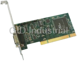
Low Profile single port asynchronous serial communication card that can be installed in any 3.3V or ...
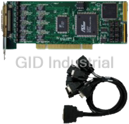
Low Profile Quad-port asynchronous RS-232serial communication card that can be installed in any 3.3V...
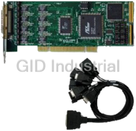
Low Profile Eight-port asynchronous RS-232 serial communication card that can be installed in any 3....
Request a Quote

The quote request has been received
Close

Facing challenges or have inquiries? Feel free to contact us!
Call Us +1-469-283-2440
What they say about us
FANTASTIC RESOURCE
One of our top priorities is maintaining our business with precision, and we are constantly looking for affiliates that can help us achieve our goal. With the aid of GID Industrial, our obsolete product management has never been more efficient. They have been a great resource to our company, and have quickly become a go-to supplier on our list!
Bucher Emhart Glass
EXCELLENT SERVICE
With our strict fundamentals and high expectations, we were surprised when we came across GID Industrial and their competitive pricing. When we approached them with our issue, they were incredibly confident in being able to provide us with a seamless solution at the best price for us. GID Industrial quickly understood our needs and provided us with excellent service, as well as fully tested product to ensure what we received would be the right fit for our company.
Fuji
HARD TO FIND A BETTER PROVIDER
Our company provides services to aid in the manufacture of technological products, such as semiconductors and flat panel displays, and often searching for distributors of obsolete product we require can waste time and money. Finding GID Industrial proved to be a great asset to our company, with cost effective solutions and superior knowledge on all of their materials, it’d be hard to find a better provider of obsolete or hard to find products.
Applied Materials
CONSISTENTLY DELIVERS QUALITY SOLUTIONS
Over the years, the equipment used in our company becomes discontinued, but they’re still of great use to us and our customers. Once these products are no longer available through the manufacturer, finding a reliable, quick supplier is a necessity, and luckily for us, GID Industrial has provided the most trustworthy, quality solutions to our obsolete component needs.
Nidec Vamco
TERRIFIC RESOURCE
This company has been a terrific help to us (I work for Trican Well Service) in sourcing the Micron Ram Memory we needed for our Siemens computers. Great service! And great pricing! I know when the product is shipping and when it will arrive, all the way through the ordering process.
Trican Well Service
GO TO SOURCE
When I can't find an obsolete part, I first call GID and they'll come up with my parts every time. Great customer service and follow up as well. Scott emails me from time to time to touch base and see if we're having trouble finding something.....which is often with our 25 yr old equipment.
ConAgra Foods